Sequential Logic
- Sequential Logic
- Introduction
- Latches and Flip-Flops
- Synchronous Logic Design
- Finite State Machines
- Timing of Sequential Logic
- Parallelism
Sequential Logic
Introduction
The outputs of sequential logic depend on both current and prior input values. Hence, sequential logic has memory. Sequential logic might explicitly remember certain previous inputs, or it might distill the prior inputs into a smaller amount of information called the state of the system. The state of a digital sequential circuit is a set of bits called state variables that contain all the information about the past necessary to explain the future behavior of the circuit.
Latches and Flip-Flops
The fundamental building block of memory is a bistable element, an element with two stable states. The figure shows a simple bistable element consisting of a pair of inverters connected in a loop. The same circuit is redrawn to emphasize the symmetry. The inverters are cross-coupled, meaning that the input of I1 is the output of I2 and vice versa. The circuit has no inputs, but it does have two outputs, and . Analyzing this circuit is different from analyzing a combinational circuit because it is cyclic: depends on , and depends on .
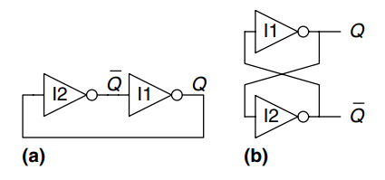
Consider the two cases, is 0 or is 1. For each case the following consequences result:
-
Case 1:
As shown in figure a), I2 receives a FALSE input, , so it produces a TRUE output on . I1 receives a TRUE input, , so it produces a FALSE output on . This is consistent with the original assumption that , so the case is said to be stable.
-
Case 2:
As shown in figure b), I2 receives a TRUE input and produces a FALSE output on . I1 receives a FALSE input and produces a TRUE output on . This is again stable.
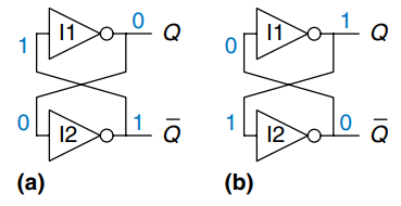
Because the cross-coupled inverters have two stable states, and , the circuit is said to be bistable. A subtle point is that the circuit has a third possible state with both outputs approximately halfway between 0 and 1. This is called a metastable state and will be discussed later.
An element with stable states conveys bits of information, so a bistable element stores one bit. The state of the cross-coupled inverters is contained in one binary state variable, . The value of tells us everything about the past that is necessary to explain the future behavior of the circuit. Specifically, if , it will remain 0 forever, and if , it will remain 1 forever. The circuit does have another node, , but does not contain any additional information because if is known, then is also known. On the other hand, is also an acceptable choice for the state variable.
When power is first applied to a sequential circuit, the initial state is unknown and usually unpredictable. it may differ each time the circuit is turned on.
Although the cross-coupled inverters can store a bit of information, they are not practical because the user has no inputs to control the state. However, other bistable elements, such as latches and flip-flops, provide inputs to control the value of the state variable.
SR Latch
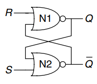
One of the simplest sequential circuits is the SR latch, which is composed of two cross-coupled gates as shown. The latch has two inputs, and , and two outputs, and . The SR latch is similar to the cross-coupled inverters, but its state can be controlled through the and inputs, which set and reset the output .
A good way to understand an unfamiliar circuit is to work out its truth table, so let’s start there. Recall that a gate produces a FALSE output when either input is TRUE. Consider the four possible combinations of and :
-
Case 1:
N1 sees at least one TRUE input, , so it produces a FALSE output on . N2 sees both and FALSE, so it produces a TRUE output on .
-
Case 2:
N1 receives inputs of 0 and . Because we don’t yet know , we can’t determine the output . N2 receives at least one TRUE input, , so it produces a FALSE output on . Now we can revisit N1, knowing that both inputs are FALSE, so the output is TRUE.
-
Case 3:
N1 and N2 both see at least one TRUE input ( or ), so each produces a FALSE output. Hence and are both FALSE.
-
Case 4:
N1 receives input of 0 and . Because we don’t yet know , we can’t determine the output. N2 receives inputs of 0 and . Because we don’t yet know , we can’t determine the output. Now we are stuck. This is reminiscent of the cross-coupled inverters. But we know that must either be 0 or 1. So we should be able to solve the problem by checking what happens in each of these subcases.
-
Case 4a:
Because and are FALSE, N2 produces a TRUE output on , as shown in a). Now N1 receives one TRUE input, , so its output, , is FALSE, just as we had assumed.
-
Case 4b:
Because is TRUE, N2 produces a FALSE output on , as shown in b). Now N1 receives two FALSE inputs, and , so its output, , is TRUE, just as we had assumed.
-
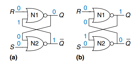
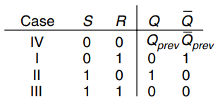
Putting this all together, suppose has some known prior value, which we shall call , before we enter Case 4. is either 0 or 1, and represents the state of the system. When and are 0, will remember this old value, and will be its complement, . The circuit has memory.
The truth table shown summarizes the four cases. The inputs and stand for Set and Reset. To set a bit means to make it TRUE. To reset a bit means to make it FALSE. The outputs, and , are normally complementary. When is asserted, is reset to 0 and does the opposite. When is asserted, is set to 1 and does the opposite. When neither input is asserted, remembers its old value, . Asserting both and simultaneously does not make much sense because it means the latch should be set and reset at the same time, which is kind of impossible. The poor circuit has no other choice but to make both outputs 0, which makes no sense.
The SR latch is represented by the symbol shown. Using the symbol is again an application of abstraction and modularity. There are various ways to build an SR latch, such as using different logic gates or transistors. Nevertheless, any circuit element with the relationship specified by the above truth table and the symbol shown is called an SR latch.
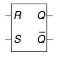
Like the cross-coupled inverters, the SR latch is a bistable element with one bit of state stored in . However, the state can be controlled through the and inputs.
D Latch
The SR latch is awkward because it behaves strangely when both inputs are asserted simultaneously. Moreover, the inputs conflate the issues of what and when. Asserting one of the inputs determines not only what the state should be but also when it should change. Circuit design becomes a lot easier when these questions are separated. The D latch in the figure solves these issues. It has two inputs. The data input, , controls what the next state should be. The clock input, , controls when the state should change.
Again, we can analyze the latch by writing the truth table, given in the figure. We notice that in all cases, is the complement of , as would seem logical. The D latch avoids the strange case of simultaneously asserted and inputs.
Putting it all together, we see that the clock controls when data flows through the latch. When , the latch is transparent. The data at flows through to as if the latch were just a buffer. When , the latch is opaque. It blocks the new data from flowing through to , and retains the old value. Hence, the D latch is sometimes called a transparent latch or a level-sensitive latch. The D latch symbol is given in c).
The D latch updates its state continuously while .

D Flip-Flop
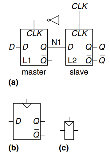
A D flip-flop can be built from two back-to-back D latches controlled by complementary clocks, as shown. The first latch, L1, is called the master. The second latch, L2, is called the slave. The node between them is named N1. Symbols for the D flip-flop are given in b) and c).
When , the master latch is transparent and the slave is opaque. Therefore, whatever value was at propagates through to N1. When , the master goes opaque and the slave becomes transparent. The value at N1 propagates through to , but N1 is cut off from . hence, whatever value was at immediately before the clock rises from 0 to 1 gets copied to immediately after the clock rises. At all other times, retains its old value, because there is always an opaque latch blocking the path between and .
In other words, a flip-flop copies to on the rising edge of the clock, and remembers its state at all other times. The rising edge of the clock is often just called the clock edge for brevity.The input specifies what the new state will be. The clock edge indicates when the state should be updated.
A D flip-flop is also known as a master-slave flip-flop, an edge-triggered flip-flop, or a positive edge-triggered flip-flop. The triangle in the symbols denotes an edge-triggered clock input.
Register
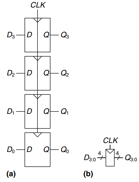
An -bit register is a bank of flip-flops that share a common input, so that all bits of the register are updated at the same time. Registers are the key building block of most sequential circuits. The figure shows the schematic and symbol for a four-bit register with inputs and outputs . and are both 4-bit busses.
Enabled Flip-Flop
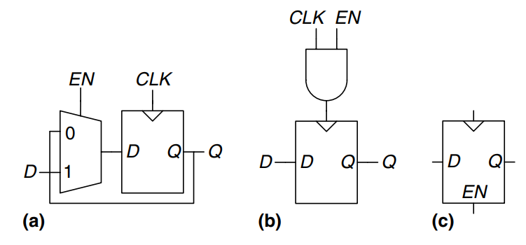
An enabled flip-flop adds another input called or ENABLE to determine whether data is loaded on the clock edge. When is TRUE, the enabled flip-flop behaves like an ordinary D flip-flop. When is FALSE, the enabled flip-flop ignores the clock and retains its state. Enabled flip-flops are useful when we wish to load a new value into the flip-flop only some of the time, rather than on every clock edge.
The figure shown two ways to construct an enabled flip-flop from a D flip-flop and an extra gate. In the first figure, an input multiplexer chooses whether to pass the value at , if is TRUE, or to recycle the old state from , if is FALSE. In the second figure, the clock is gated. If is TRUE, the input to the flip-flop toggles normally. If is FALSE, the input is also FALSE and the flip-flop retains its old value. Notice that must not change while , lest the flip-flop see a clock glitch. Generally, performing logic on the clock is a bad idea. Clock gating delays the clock and can cause timing errors, as we will see later.
Resettable Flip-Flop
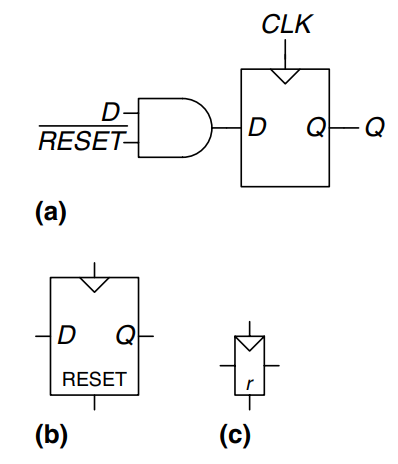
A resettable flip-flop adds another input called . When is FALSE, the resettable flip-flop behaves like an ordinary D flip-flop. When is TRUE, the resettable flip-flop ignores and resets the output to 0. Resettable flip-flops are useful when we want to force a known state into all the flip-flops in a system when we first turn it on.
Such flip-flops may be synchronously or asynchronously resettable. Synchronously resettable flip-flops reset themselves only on the rising edge of the clock. Asynchronously resettable flip-flops reset themselves as soon as becomes TRUE, independent of the clock.
The figure shows how to construct a synchronously resettable flip-flop from an ordinary D flip-flop and an gate.
Asynchronously resettable flip-flops require modifying the internal structure of the flip-flop.
As one might imagine, settable flip-flops are also occasionally used. They load a 1 into the flip-flop when is asserted, and they too come in synchronous and asynchronous flavors. Resettable and settable flip-flops may also have an enable input and may be grouped into -bit registers.
Transistor-Level Latch and Flip-Flop Designs
Latches and flip-flops require a large number of transistors when built from logic gates. But the fundamental role of a latch is to be transparent or opaque, much like a switch. Recall from Introduction that a transmission gate is an efficient way to build a CMOS switch, so we might expect that we could take advantage of transmission gates to reduce the transistor count.
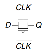
A compact D latch can be constructed from a single transmission gate, as shown.
This latch suffers from two major limitations:
- floating output node: when the latch is opaque, is not held at its value by any gates. This is called a floating or dynamic node. After some time, noise and charge leakage may disturb the value of .
- no buffers: the lack of buffers has caused malfunctions on several commercial chips. A spike of noise that pulls to a negative voltage can turn on the nMOS transistor, making the latch transparent, even when . Likewise, a spike on above can turn on the pMOS transistor even when . And the transmission gate is symmetric, so it could be driven backward with noise on affecting the input . The general rule is that neither the input of a transmission gate nor the state node of a sequential circuit should ever be exposed to the outside world, where noise is likely.
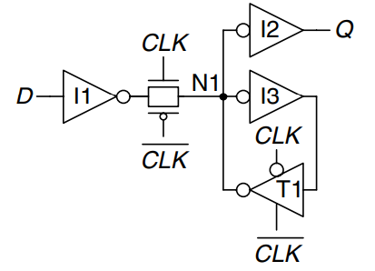
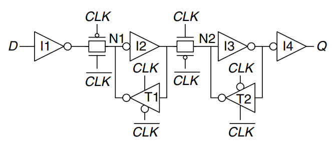
The figure shows a more robust 12-transistor D latch used on modern commercial chips. It is still built around a clocked transmission gate, but it adds inverters I1 and I2 to buffer the input and output. The state of the latch is held on node N1. Inverter I3 and the tristate buffer T1 provide feedback to turn N1 into a static node. If a small amount of noise occurs on N1 while , T1 will drive N1 back to a valid logic value.
The figure shows a D flip-flop constructed from two static latches controlled by and . Some redundant internal inverters have been removed, so the flip-flop requires only 20 transistors.
Synchronous Logic Design
In general, sequential circuits include all circuits that are not combinational - that is, those whose output cannot be determined by simply looking at the current inputs.
Unstable Circuits
This circuit, where three inverters are routed in series, feeding the output back as the input, is an example of an unstable circuit.
Assume node is 0 initially. Then , and hence , which is inconsistent with out initial assumption. The circuit has no stable state and is said to be unstable or astable.

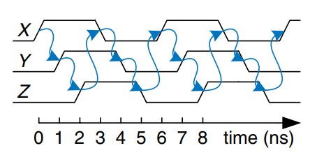
Assume each inverter has a propagation delay of 1 ns. Then the timing diagram of the circuit looks as shown. Each node oscillates between 0 and 1 with a period of 6 ns. This circuit is called a ring oscillator.
Race Conditions
Let’s examine a new D latch design with fewer gates.
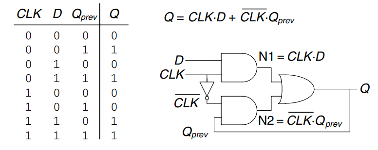
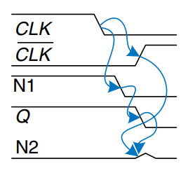
This circuit has a race condition, as can be seen from the timing diagram shown. This race condition causes it to fail when certain gates are slower than others. Suppose . The latch is transparent and passes through to make . Now, falls. The latch should remember its old value, keeping . However, suppose the delay through the inverter from to is rather long compared to the delays of the and gates. Then nodes N1 and may both fall before rises. In such a case, N2 will never rise, and becomes stuck at 0.
This is an example of an asynchronous circuit design in which outputs are directly fed back to inputs. Asynchronous circuits are infamous for having race conditions where the behavior of the circuit depends on which of two paths through logic gates is fastest. One circuit may work, while a seemingly identical one built from gates with slightly different delays may not work. Or the circuit may work only at certain temperatures or voltages at which the delays are just right. These mistakes are extremely difficult to track down.
Synchronous Sequential Circuits
The previous two examples contain loops called cyclic paths, in which outputs are fed directly back to inputs. They are sequential rather than combinational circuits. Combinational logic has no cyclic paths and no races. If inputs are applied to combinational logic, the outputs will always settle to the correct value within a propagation delay. However, sequential circuits with cyclic paths can have undesirable races or unstable behavior.
To avoid these problems, designers break the cyclic paths by inserting registers somewhere in the path, This transforms the circuit into a collection of combinational logic and registers. The registers contain the state of the system, which changes only at the clock edge, so we say the state is synchronized to the clock. If the clock is sufficiently slow, so that the inputs to all registers settle before the next clock edge, all races are eliminated. Adopting this discipline of always using registers in the feedback path leads us to the formal definition of a synchronous sequential circuit.
Recall that a circuit is defined by its input and output terminals and its functional and timing specifications. A sequential circuit has a finite set of discrete states . A synchronous sequential circuit has a clock input, whose rising edges indicate a sequence of times at which state transitions occur. We often use the terms current state and next state to distinguish the state of the system at the present from the state to which it will enter on the next clock edge. The functional specification details the next state and the value of each output for each possible combination of current state and input values. The timing specification consists of an upper bound, , and a lower bound, , on the time from the rising edge of the clock until the output changes, as well as setup and hold times, and , that indicate when the inputs must be stable relative to the rising edge of the clock.
The rules of synchronous sequential circuit composition teach us that a circuit is a synchronous sequential circuit if it consists of interconnected circuit elements such that
- every circuit element is either a register or a combinational circuit
- at least one circuit element is a register
- all registers receive the same clock signal
- every cyclic path contains at least one register
Sequential circuits that are not synchronous are called asynchronous.
A flip-flop is the simplest synchronous sequential circuit, as shown.
We often call the current state variable and the next state variable .
Two other common types of synchronous sequential circuits are called finite state machines and pipelines.
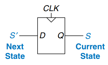
Synchronous and Asynchronous Circuits
Asynchronous design in theory is more general than synchronous design, because the timing of the system is not limited by clocked registers. Just as analog circuits are more general than digital circuits because analog circuits can use any voltage, asynchronous circuits are more general than synchronous circuits because they can use any kind of feedback. However, synchronous circuits have proved to be easier to design and use than asynchronous circuits, just as digital are easier than analog circuits. Despite decades of research on asynchronous circuits, virtually all digital systems are essentially synchronous.
Of course, asynchronous circuits are occasionally necessary when communicating between systems with different clocks or when receiving inputs at arbitrary times, just as analog circuits are necessary when communicating with the real world of continuous voltages. Furthermore, research in asynchronous circuits continues to generate interesting insights, some of which can improve synchronous circuits too.
Finite State Machines
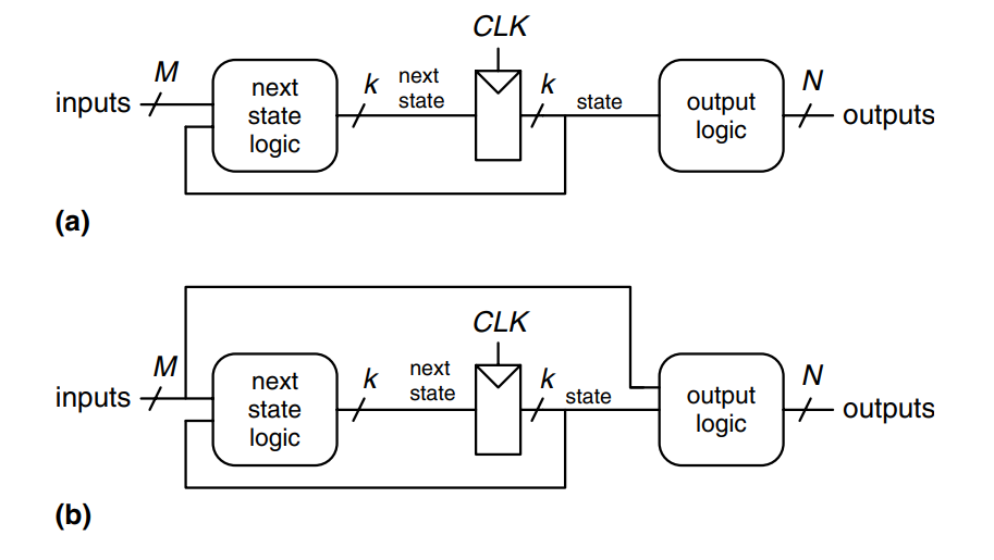
Synchronous sequential circuits can be drawn in the forms shown in the figure. These forms are called finite state machines (FSMs). They get their name because a circuit with registers can be in one of a finite number () unique states. An FSM has inputs, outputs, and bits of state. It also receives a clock and, optionally, a reset signal. An FSM consists of two blocks of combinational logic, next state logic and output logic, and a register that stores the state. On each clock edge, the FSM advances to the next state, which was computed based on the current state and inputs. There are two general classes of finite state machines, characterized by their functional specifications. In Moore machines (a)), the outputs depend only on the current state of the machine. In Mealy machines (b)), the outputs depend on both the current state and the current inputs. Finite state machines provide a systematic way to design synchronous sequential circuits given a functional specification.
FSM Design Example
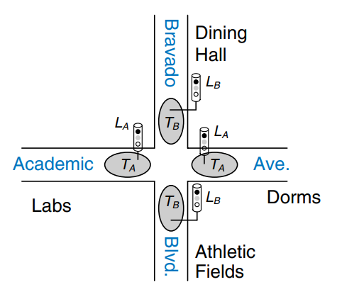
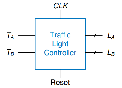
Consider the problem of inventing a controller for a traffic light at a busy intersection. We install two traffic sensors, and , on both roads each. Each sensor indicates TRUE if someone is present and FALSE if the street is empty. We also install two traffic lights, and , to control traffic. Each light receives digital inpputs specifying whether it should be green, yellow or red. Hence, this FSM should have two inputs, and , and two outputs, and . The intersection with lights and sensors is shown in the figure. We provide a clock with a 5-second period. On each clock tick, the lights may change based on the traffic sensors. We also provide a reset button so that we can put the controller in a known initial state when turning it on.
A black box view of the state machine could look as shown.
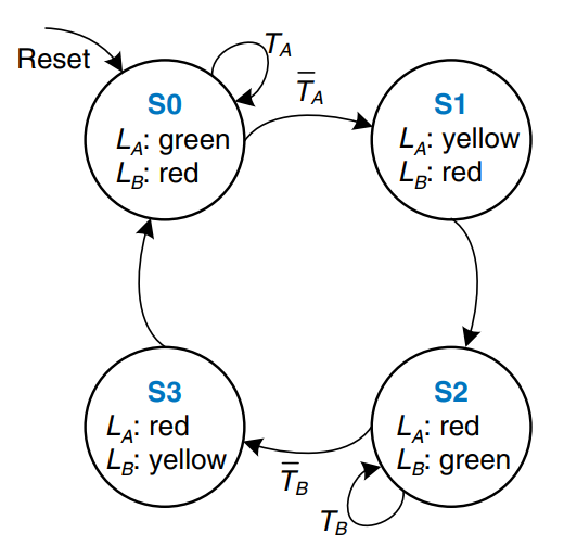
We can sketch a state transition diagram, as shown, to indicate all the possible states of the system and the transitions between those states.
In a state transition diagram, circles represent states and arcs represent transitions between states. The transitions take place on the rising edge of the clock; we do not bother to show the clock on the diagram, because it is always present in a synchronous sequential circuit. Moreover, the clock simply controls when the transitions should occur, whereas the diagram indicates which transitions occur. The arc labeled Reset pointing from outer space into state S0 indicates that the system should enter that state upon reset, regardless of what previous state it was in. If a state has multiple arcs leaving it, the arcs are labeled to show what input triggers each transition. If a state has a single transition leaving it, that transition always occurs regardless of the inputs.
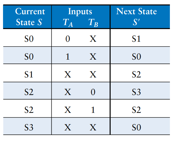
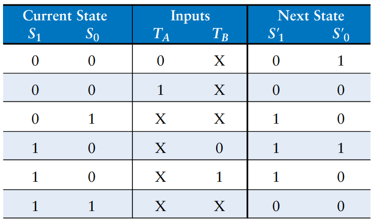
We can also rewrite this state transition diagram as a state transition table, which indicates, for each state and input, what the next state, should be, as shown. Note that Reset is omitted from the table. Instead, we use resettable flip-flops that always to to state S0 on reset, independent of the inputs.
The state transition diagram is abstract in that it uses states labeled S0 through S3 and outputs labeled after their respective color. To build a real circuit, the states and outputs must be assigned binary encodings.
We choose simple encodings as shown.
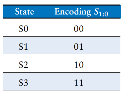
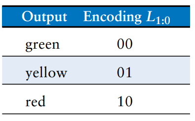
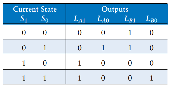
We update the state transition table to use these binary encodings, as shown. The revised state transition table is a truth table specifying the next state logic. It defines next state, , as a function of the current state, , and the inputs. The revised output table is a truth table specifying the output logic. It defines the outputs, and , as functions of the current state, .
From this table, it is straightforward to read off the Boolean equations for the next state in sum-of-products from.
The equations can be simplified further. We can then see that reduces to an operation. The next state equations are as follows:
Similarly, we can write an output table indicating, for each state, what the output should be in that state. Again, its straightforward to read off and simplify the Boolean equations for the outputs. For example, observe that is TRUE only on the rows where is TRUE.
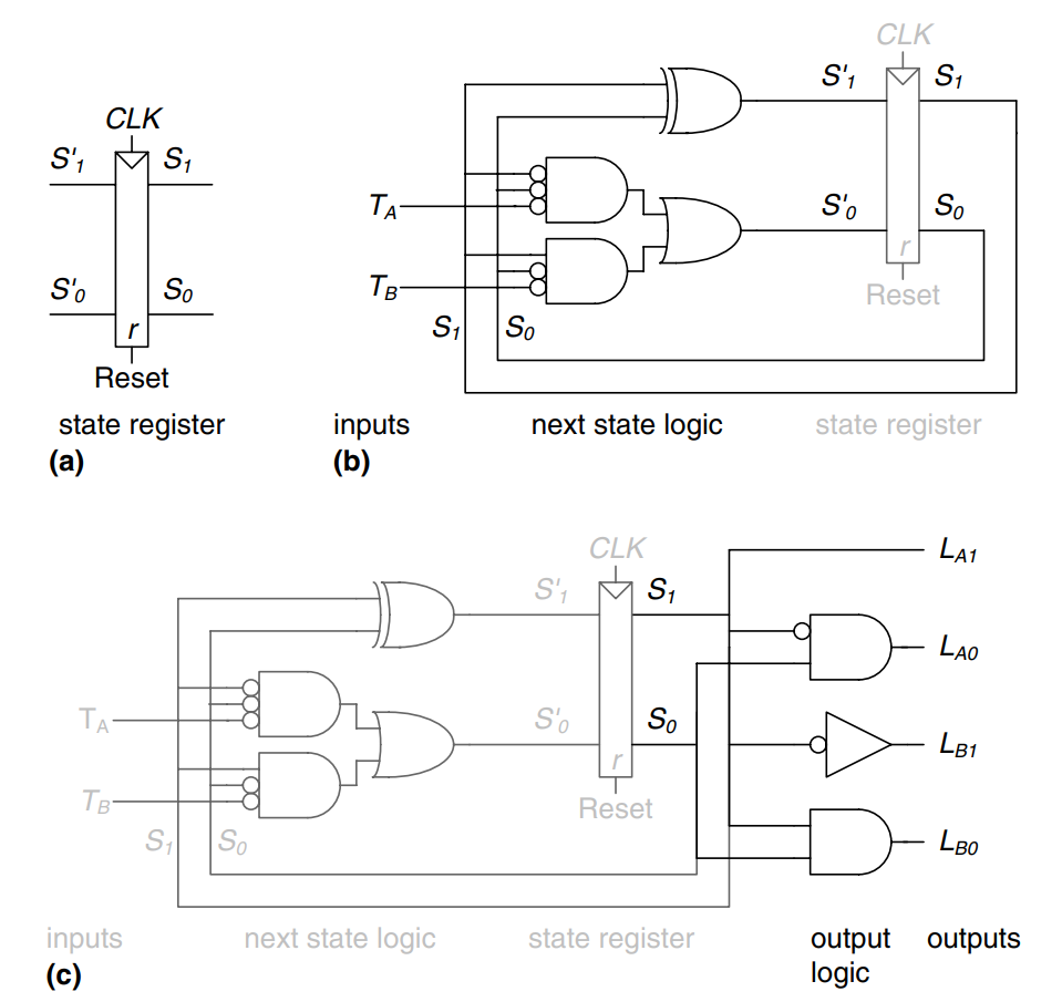
Finally, we can draw our Moore FSM. First, we draw the 2-bit state register as shown in a). On each clock edge, the state register copies the next state, , to become the state, . The state register receives a synchronous or asynchronous reset to initialize the FSM at startup. Then, we draw the next state logic, based on the above equations, which computes the next state, based on the current state and inputs, as shown in b). Finally, we draw the output logic, based on above equations, which computes the outputs based on the current state, as shown in c).
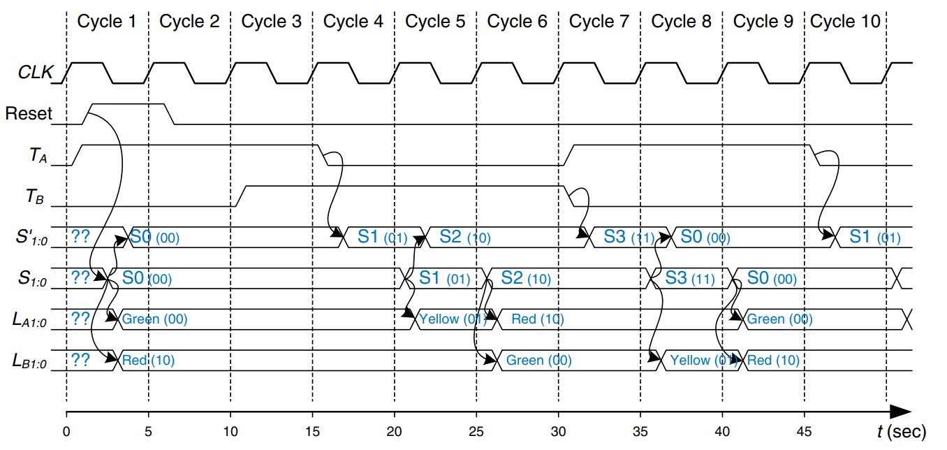
The figure shows a timing diagram illustrating the traffic light controller going through a sequence of states. The diagram shows , Reset, the inputs and , next state , state , and outputs and . Arrows indicate causality.
The clock has a 5-second period, so the traffic lights change at most once every 5 seconds. When the finite state machine is first turned on, its state is unknown, as indicated by the question marks. Therefore, the system should be reset to put it into a known state. In this timing diagram, immediately resets to S0, indicating that asynchronously resettable flip-flops are being used.
State Encodings
In the previous example, the state and output encodings were selected arbitrarily. A natural question is how to determine the encoding that produces the circuit with the fewest logic gates or the shortest propagation delay. Unfortunately, there is no simple way to find the best encoding except to try all possibilities, which is infeasible if the number of states is large.
One important decision in state encoding is the choice between binary encoding and one-hot encoding. With binary encoding, as was used in the traffic light controller example, each state is represented as a binary number. Because binary numbers can be represented by bits, a system with states only needs bits of state.
In one-hot encoding, a separate bit of state is used for each state. It is called one-hot because only one bit is “hot” or TRUE at any time. Each bit of state is stored in one flip-flop, so one-hot encoding requires more flip-flops than binary encoding. However, with one-hot encoding, the next-state and output logic is often simpler, so fewer gates are required.
A related encoding is the one-cold encoding, in which states are represented with bits, exactly one of which is FALSE.
Moore and Mealy Machines
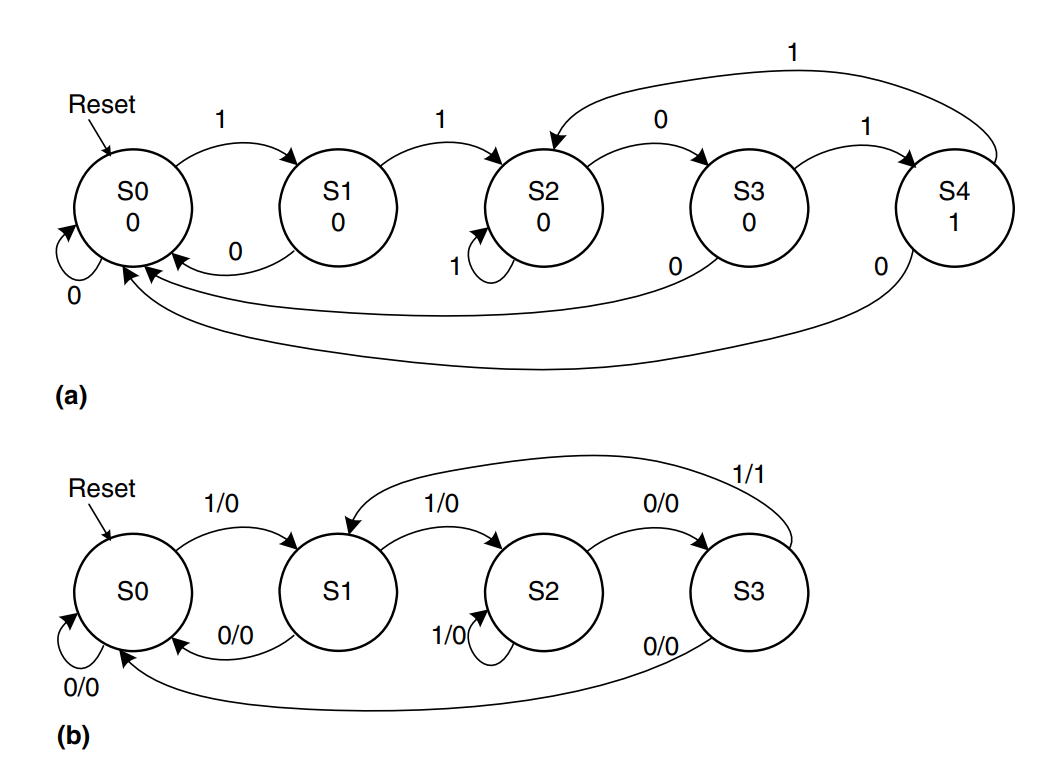
In Moore machines the output depends only on the state of the system. Hence, in state transition diagrams for Moore machines, the outputs are labeled in the circles. Recall that Mealy machines are much like Moore machines, but the outputs can depend on inputs as well as the current state. Hence, in state transition diagrams for Mealy machines, the outputs are labeled on the arcs instead of in the circles. The block of combinational logic that computes the outputs uses the current state and inputs, as shown in the schematic of a Mealy machine above.
Example state transition diagrams for Moore (a)) and Mealy (b)) machines are shown.
Factoring State Machines
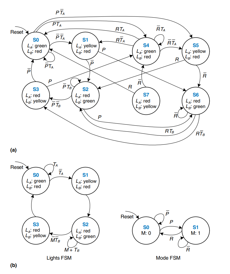
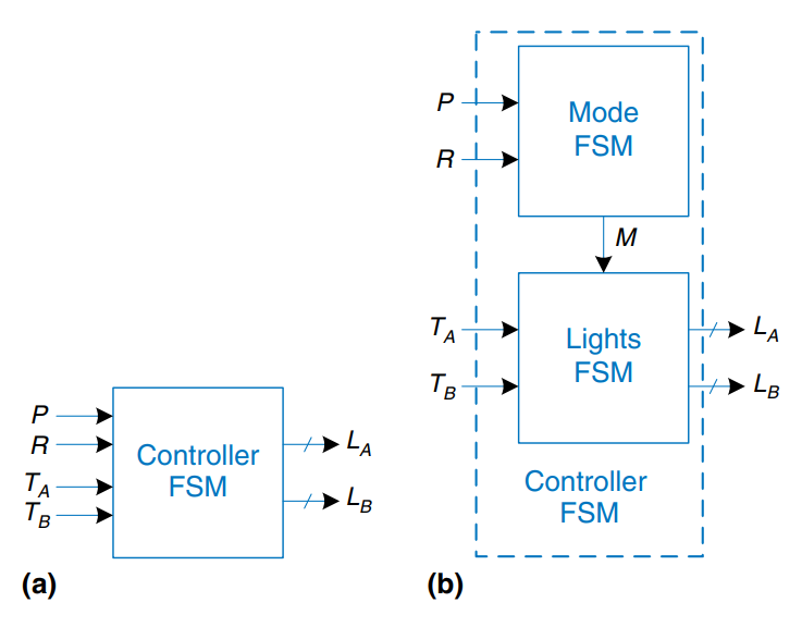
Designing complex FSMs is often easier if they can be broken down into multiple interacting simpler state machines such that the output of some machines is the input of others. This application of hierarchy and modularity is called factoring of state machines.
As shown in the diagrams, where a) is the unfactored, and b) the factored version of the same circuit.
FSM Review
Finite state machines are a powerful way to systematically design sequential circuits from a written specification. Use the following procedure to design an FSM:
- identify the inputs and outputs
- sketch a state transition diagram
- for a Moore machine:
- write a state transition table
- write an output table
- for a Mealy machine:
- write a combined state transition and output table
- select state encodings - selection affects the hardware design
- write Boolean equations for the next state and output logic.
- sketch the circuit schematic
Timing of Sequential Logic
Recall that a flip-flop copies the input to the output on the rising edge of the clock. This process is called sampling on the clock edge. If is stable at either 0 or 1 when the clock rises, this behavior is clearly defined. But what happens if is changing at the same time the clock rises?
This problem is similar to that faced by a camera when snapping a picture. Imagine photographing a frog jumping from a lily pad into the lake. If you take the picture before the jump, you will see a frog on a lily pad. If you take the picture after the jump, you will see ripples in the water. But if you take it just as the frog jumps, you may see a blurred image of the frog stretching from the lily pad into the water. A camera is characterized by its aperture time, during which the object must remain still for a sharp image to be captured. Similarly, a sequential element has an aperture time around the clock edge, during which the input must be stable for the flip-flop to produce a well-defined output.
The aperture of a sequential element is defined by a setup and a hold time, before and after the clock edge, respectively. just as the static discipline limited us to using logic levels outside the forbidden zone, the dynamic discipline limits us to using signals that change outside the aperture time, By taking advantage of the dynamic discipline, we can think of time in discrete units called clock cycles, just as we think of signal levels as discrete 1’s and 0’s. A signal may glitch and oscillate wildly for some bounded amount of time. Under the dynamic discipline we are concerned only about its final value at the end of the clock cycle, after it has settled to a stable value. Hence we can simply write , the value of signal at the end of the -th clock cycle, where is an integer, rather than , the value of at some instant , where is a real number.
The clock period has to be long enough for all signals to settle. This sets a limit on the speed of the system. In real systems, the clock does not reach all flip-flops at precisely the same time. This variation in time, called clock skew, further increases the necessary clock period.
Sometimes it is impossible to satisfy the dynamic discipline, especially when interfacing with the real world. For example, consider a circuit with an input coming from a button. One might press the button just as the clock rises. This can result in a phenomenon called metastability, where the flip-flop captures a value partway between 0 and 1 that can take an unlimited amount of time to resolve into a good logic value. The solution to such asynchronous inputs is to use a synchronizer, which has a very small (but nonzero) probability of producing an illegal logic value.
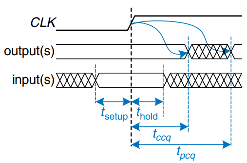
The Dynamic Discipline
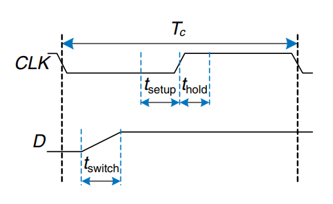
So far, we have focused on the functional specification of sequential circuits. Recall that a synchronous sequential circuit, such as a flip-flop or FSM, also has a timing specification, as shown. When the clock rises, the output(s) may start to change after the clock-to- contamination delay, , and must definitely settle to the final value within the clock-to- propagation delay, . These represent the fastest and slowest delays through the circuit, respectively. For the circuit to sample its input correctly, the input(s) must have stabilized at least some setup time, , before the rising edge of the clock and must remain stable for at least some hold time, , after the rising edge of the clock. The sum of the setup and hold times is called the aperture time of the circuit, because it is the total time for which the input must remain stable.
The dynamic discipline states that the inputs of a synchronous sequential circuit must be stable during the setup and hold aperture time around the clock edge. By imposing this requirement, we guarantee that the flip-flops sample signals while they are not changing. Because we are concerned only about the final values of the inputs at the time they are sampled, we can treat signals as discrete in time as well as in logic levels.
System Timing
The clock period or cycle time, , is the time between rising edges of a repetitive clock signal. Its reciprocal, , is the clock frequency. All else being the same, increasing the clock frequency increases the work that a digital system can accomplish per unit time. Frequency is measured in units of Hertz (Hz), or cycles per second.
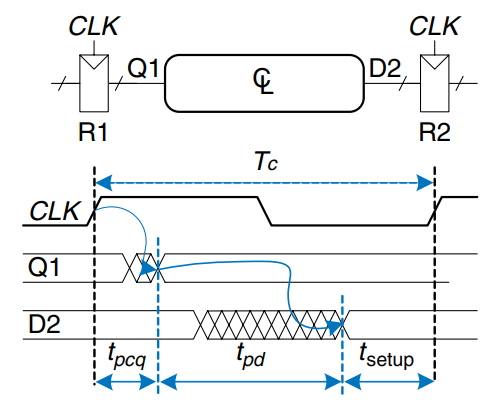
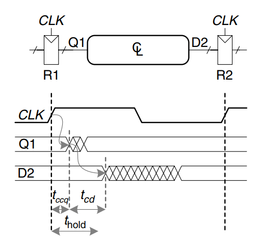
The figure a) illustrates a generic path in a synchronous sequential circuit whose clock period we wish to calculate. On the rising edge of the clock, register R1 produces output(s) 1. These signals enter a block of combinational logic, producing 2, the input(s) to register R2. The timing diagram in b) shows that each output signal may start to change a contamination delay after its input changes and settles to the final value withing a propagation delay after its input settles. The gray arrows represent the contamination delay through R1 and the combinational logic, the blue arrows represnt the propagation delay through R1 and the combinational logic. We analyze the timing constraints with respect to the setup and hold time of the second register, R2.

Setup Time Constraint
The figure shows the timing diagram with only the maximum delay through the path, indicated by the blue arrows. To satisfy the setup time of R2, 2 must settle no later than the setup time before the next clock edge. hence, we find an equation for the minimum clock period:
In commercial designs, the clock period is often dictated by the Director of Engineering or by the marketing department to ensure a competitive product. Moreover, the flip-flop clock-to- propagation delay and setup time, and , are specified by the manufacturer. Hence, we can rearrange above equation to solve for the maximum propagation delay through the combinational logic, which is usually the only variable under the control of the designer. c
The term in parentheses, , is called the sequencing overhead. Ideally, the entire cycle time, , would be available for useful computation in the combinational logic, . However, the sequencing overhead of the flip-flop cuts into this time. This equation is called the setup time constraint or max-delay constraint, because it depends on the setup time and limits the maximum delay through combinational logic.
If the propagation delay through the combinational logic is too great, 2 may not have settled to its final value by the time R2 needs it to be stable and samples it. Hence, R2 may sample an incorrect result or even an illegal logic level, a level in the forbidden region. In such a case, the circuit will malfunction. The problem can be solved by increasing the clock period or redesigning the combinational logic to have a shorter propagation delay.
Hold Time Constraint
The register R2 also has a hold time constraint. Its input, 2, must not change until some time, , after the rising edge of the clock. According to the figure, 2 might change as soon as after the rising edge of the clock. Hence, we find
Again, and are characteristics of the flip-flop that are usually outside the designer’s control. Rearranging, we can solve for the minimum contamination delay through the combinational logic:
This equation is also called the min-delay constraint because it limits the minimum delay through combinational logic.
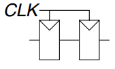
We have assumed that any logic elements can be connected to each other without introducing timing problems. In particular, we would expect that two flip-flops may be directly cascaded as in the figure without causing hold time problems. In particular, we would expect that two flip-flops may be directly cascaded as shown without causing hold time problems.
In such a case, because there is no combinational logic between flop-flops. Substituting into the above equation yields the requirements that
In other words, a reliable flip-flop must have a hold time shorter than its contamination delay. Often, flip-flops are designed with , such that this inequality is always satisfied. Unless noted otherwise, we will usually make that assumption and ignore the hold time constraint.
Nevertheless, hold time constraints are critically important. If they are violated, the only solution is to increase the contamination delay through the logic, which requires redesigning the circuit. Unlike setup time constraints, they cannot be fixed by adjusting the clock period, so hold time violations must be taken seriously.
Putting It All Together
Sequential circuits have setup and hold time constraints that dictate the maximum and minimum delays of the combinational logic between flip-flops. Modern flip-flops are usually designed so that the minimum delay through the combinational logic is 0 - that is, flip-flops can be places back-to-back. The maximum delay constraint limits the number of consecutive gates on the critical path of a high-speed circuit, because a high clock frequency means a short clock period.
Clock Skew
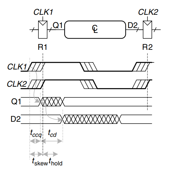
In the previous analysis, we assumed that the clock reaches all registers at exactly the same time. In reality, there is some variation in this time. This variation in clock edges is called clock skew. For example, the wires from the clock source to different registers may be of different lengths, resulting in slightly different delays, as shown. Noise also results in different delays. Clock gating further delays the clock. If some clocks are gated and others are not, there will be substantial skew between the gated and ungated clocks. In the figure, 2 is early with respect to 1, because the clock wire between the two registers follows a scenic route. When doing timing analysis, we consider the worst-case scenario, so that we can guarantee that the circuit will work under all circumstances.
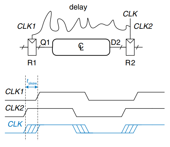
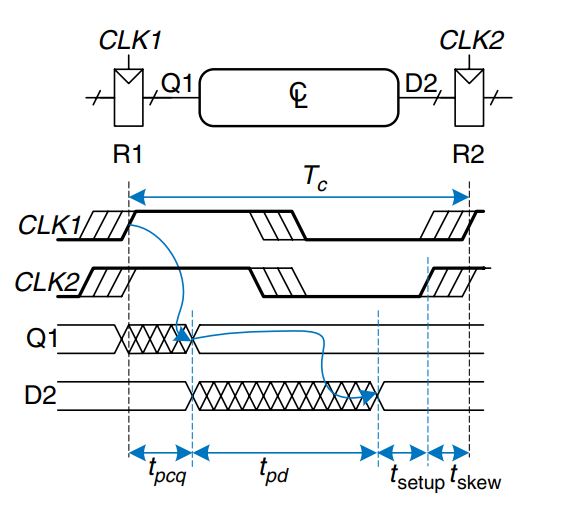
This figure adds skew to the timing diagram from the setup time constraints section. The heavy clock line indicates that the latest time at which the clock signal might reach any register; the hashed lines show that the clock might arrive up to earlier.

First, consider the setup time constraint shown in the figure. In the worst case, R1 receives the latest skewed clock and R2 receives the earliest skewed clock, leaving as little time as possible for data to propagate between the registers.
The data propagates through the registers and combinational logic and must setup before R2 samples it. Hence, we conclude that
Next, consider the hold time constraint shown in the figure. In the worst case, R1 receives an early skewed clock, 1, and R2 receives a late skewed clock, 2. The data zips through the register and combinational logic but must not arrive until a hold time after the late clock. Thus, we find that
In summary, clock skew effectively increases both the setup time and the hold time. It adds to the sequencing overhead, reducing the time available for useful work in the combinational logic. It also increases the required minimum delay through the combinational logic. Even if , a pair of back-to-back flip-flops will violate the latter of the above equations if . To prevent serious hold time failures, designers must not permit too mmuch clock skew. Sometimes flip-flops are intentionally designed to be particularly slow (i.e., large ), to prevent hold time problems even when the clock skew is substantial.
Metastability
As noted earlier, it is not always possible to guarantee that the input to a sequential circuit is stable during the aperture time, especially when the input arrives from the external world. Consider a button connected to the input of a flip-flop as shown. When the button is not pressed, . When the button ispressed, . One presses the button at some random time relative to the rising edge of . We want to know the output after the rising edge of . In case 1, when the button is pressed much before , .
In case 2, when the button is not pressed until long after , . But in case 3, when the button is pressed sometime between before and after , the input violates the dynamic discipline and the output is undefined.
Metastable State
In reality, when a flip-flop samples an input that is changing during its aperture, the output may momentarily take on a voltage between 0 and that is in the forbidden zone. This is called a metastable state. Eventually, the flip-flop will resolve the output to a stable state of either 0 or 1. However, the resolution time required to reach the stable state is unbounded.
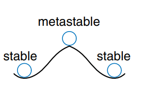
The metastable state of a flip-flop is analogous to a ball on the summit of a hill between two valleys, as shown. the two valleys are stable states, because a ball in the valley will remain there as long as it is not disturbed. The top of the hill is called metastable because the ball would remain there if it were perfectly balanced. But because nothing is perfect, the ball will eventually roll to one side or the other. The time required for this change to occur depends on how nearly well balanced the ball originally was. Every bistable device has a metastable state between the two stable states.
Resolution Time
If a flip-flop input changes at a random time during the clock cycle, the resolution time, , required to resolve to a stable state is also a random variable. If the input changes outside the aperture, then . But if the input happens to change withing the aperture, can be substantially longer. Theoretical and experimental analyses have shown that the probabilit that the resolution time exceeds some arbitrary time decreases exponentially with : r
where is the clock period, and and are characteristics of the flip-flop. The equation is valid only for substantially longer than .
Intuitively, describes the probability that the input changes at a bad time (i.e., during the aperture time); this probability decreases with the cycle time, . is a time constant indicating how fast the flip-flop moves away from the metastable state;it is related to the delay through the cross-coupled gates in the flip-flop.
In summary, if the input to a bistable device such as a flip-flop changes during the aperture time, the output may take on a metastable value for some time before resolving to a stable 0 or 1. The amount of time required to resolve is unbounded, because for any finite time the probability that the flip-flop is still metastable is nonzero. However, this probability drops off exponentially as increases. Therefore, if we wait long enough, much longer than , we can expect with exceedingly high probability that the flip-flop will reach a valid logic level.
Synchronizers
Asynchronous inputs to digital systems from the real world are inevitable. Human input is asynchronous, for example. If handled carelessly, these asynchronous inputs can lead to metastable voltages within the system, causing erratic system failures that are extremely difficult to track down and correct. The goal of a digital system designer should be to ensure that, given asynchronous inputs, the probability of encountering a metastable voltage is sufficiently small. “Sufficiently” depends on the context. For a digital cell phone, perhaps one failure in 10 years is acceptable, because the user can always turn the phone off and back on if it locks up. For a medical device, one failure in the expected life of the universe ( years) is a better target :). To guarantee good logic levels, all asynchronous inputs should be passed through synchronizers.
A synchronizer, as shown, is a device that receives an asynchronous input, , and a clock, . It produces an output, , within a bounded amount of time; the output has a valid logic level with extremely high pobability. If is stable during the aperture, should take on the same value as . If changes during the aperture, may take on either a HIGH or LOW value but must not be metastable.
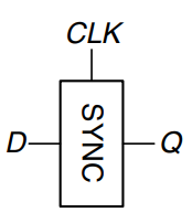
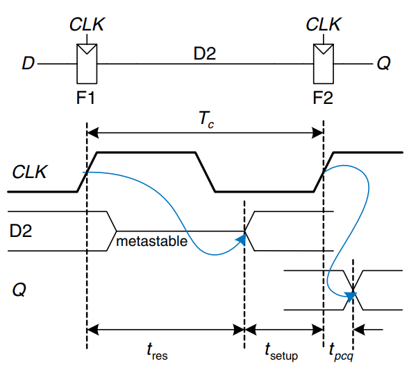
The figure shows a simple way to build a synchronizer out of two flip-flops. F1 samples on the rising edge of . If is changing at that time, the output D2 may be momentarily metastable. If the clock period is long enough, D2 will, with high probability,resolve to a valid logic level before the end of the period. F2 then samples D2, which is now stable, producing a good output .
We say that a synchronizer fails if , the output of the synchronizer, becomes metastable.This may happen if D2 has not resolved to a valid level by the time it must setup at F2- that is, if . According to the above equation, the probability of failure for a single input change at a random time is
The probability of failure, , is the probability that the output, , will be metastable upon a single change in . If changes once per second, the probability of failure per second is given by that. However, if changes times per second, the probability of failure per second is times as great:
System reliability is usually measured in mean time between failures (MTBF). As the name suggest, MTBF is the average amount of time between failures of the system. It is the reciprocal of the probability that the system will fail in any given second
This equation shows that the MTBF improves exponentially as the synchronizer waits for a longer time, . For most systems, a synchronizer that waits for one clock cycle provides a safe MTBF. In exceptionally high-speed systems, waiting for more cycles may be necessary.
Derivation of Resolution Time
The equation for the probability of failure at any given time can be derived using a basic knowledge of circuit theory, differential equations, and probability.
A flip-flop output will be metastable after some time, , if the flip-flop samples a changing input (causing a metastable condition) and the output does not resolve to a valid level within that time after the clock edge. Symbolically, this can be expressed as
We consider each probability term individually. The asynchronous input signal switches between 0 and 1 in some time, , as shown in the figure. The probability that the input changes during the aperture around the clock edge is
If the flip-flop does enter metastability - that is, with probability - the time to resolve from metastability depends on the inner workings of the circuit. This resolution time determines , the probability that the flip-flop has not yet resolved to a valid logic level after a time .
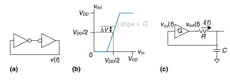
A bistable device uses storage with positive feedback. Figure a) shows this feedback implemented with a pair of inverters; this circuit’s behavior is representative of most bistable elements. A pair of inverters behaves like a buffer. Let us model it as having the symmetric DC transfer characteristics shown in b), with a slope of . The buffer can deliver only a finite amount of output current; we can model this as an output resistance, . All real circuits also have some capacitance, , that must be charged up. Charging the capacitor through the resistor causes an RC delay, preventing the buffer from switching instantaneously. Hence, the complete circuit model is shown in c), where is the voltage of interest conveying the state of the bistable device.
The metastable point for this circuit is ; if the circuit began at exactly that point, it would remain there indefinitely in the absence of noise. Because voltages are continuous variables, the cance that the circuit will begin at exactly the metastable point is vanishingly small. However, the circuit might begin at time 0 near metastability at for some small offset . In such a case, the positive feedback will eventually drive to if and to 0 if . The time required to reach or 0 is the resolution time of the bistable device.
The DC transfer characteristic is nonlinear, but it appears linear near the metastable point, which is the region of interest to us. Specifically, if , then for small . The current through the resistor is . The capacitor charges at a rate . Putting these facts together, we find the governing equation for the output voltage.
This is a linear first-order differential equation. Solving it with the initial condition gives
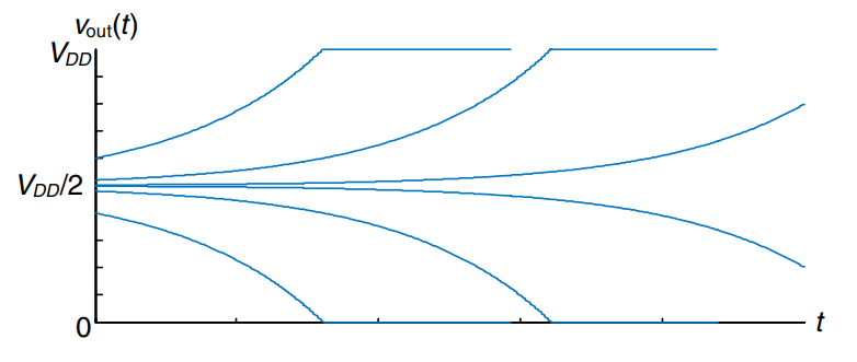
The figure plots trajectories for given various starting points. moves exponentially away from the metastable point until it saturates at or 0. The output voltage eventually resolves to 1 or 0. The amount of time this takes depends on the initial voltage offset () from the metastable point ().
Solving the above equation for the resolution time , such that or , gives
In summary, the resolution time increases if the bistable device has high resistance or capacitance that causes the output to change slowly. It decreases if the bistable device has high gain, . The resolution time also increases logarithmically as the circuit starts closer to the metastable point ().
Define as . Solving the above equation for finds the initial offset, , that gives a particular resolution time, :
Suppose that the bistable device samples the input while it is changing. It measures a voltage, , which we will assume is uniformly distributed between 0 and . The probability that the output has not resolved to a legal value after time depends on the probability that the initial offset is sufficiently small. Specifically, the initial offset on must be less than , so the initial offset on must be less than . Then the probability that the bistable device samples the input at a time to obtain a sufficiently small initial offset is
Putting this all together, the probability that the resolution time exceeds some time, , is given by the following equation:
Observe that this equation is in the same form of the original equation, where and . In summary, we have derived the original statement and shown how and depend on physical properties of the bistable device.
Parallelism
The speed of a system is measured in latency and throughput of tokens moving through a system. We define a token to be a group of inputs that are processed to produce a group of outputs. The latency of a system is the time required for one token to pass through the system from start to end. The throughput is the number of tokens that can be produced per unit time.
The throughput can be improved by processing several tokens at the same time. This is called parallelism, and it comes in two forms: spatial and temporal. With spatial parallelism, multiple copies of the hardware are provided so that multiple tasks can be done at the same time. With temporal parallelism, a task is broken into stages, like an assembly line. Multiple tasks can be spread across the stages. Although each task must pass through all stages, a different task will be in each stage at any given time so multiple tasks can overlap. Temporal parallelism is commonly called pipelining.
Consider a task with latency . In a system with no parallelism, the throughput is . In a spatially parallel system with copies of the hardware, the throughput is . In a temporally parallel system, the task is ideally broken into steps, or stages, of equal length. In such a case, the thtoughput is also , and only one copy of the hardware is required. However, finding steps of equal length is often impractical. If the longest step as a latency , the pipelined throughput is .
Pipelining is particularly attractive because it speeds up a circuit without duplicating the hardware. Instead, registers are placed between blocks of combinational logic to divide the logic into shorter stages that can run with a faster clock. The registers prevent a token in one pipeline stage from catching up with and corrupting the token in the next stage.
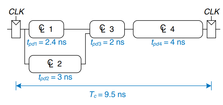
The figure shows an example of a circuit with no pipelining. It contains four blocks of logic between the registers. The critical path passes through blocks 2, 3, and 4. Assume that the register has a clock-to- propagation delay of 0.3 ns and a setup time of 0.2 ns. Then the cycle time is . The circuit has a latency of 9.5 ns and a throughput of .
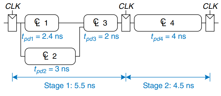
This figure shows the same circuit partitioned into a two-stage pipeline by adding a register between blocks 3 and 4. The first stage has a minimum clock period of . The second stage has a minimum clock period of . The clock must be slow enough for all stages to work. Hence, . The latency is two clock cycles, or . The throughput is . This example shows that, in a real circuit, pipelining with two stages almost doubles the throughput and slightly increases the latency. In comparison, ideal pipelining would exactly double the throughput at no penalty in latency. The discrepancy comes about because the circuit cannot be divided into two exactly equal halves and because the registers introduce more sequencing overhead.
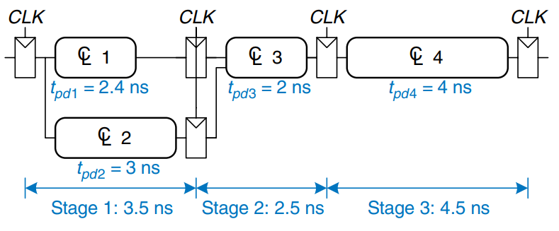
The figure shows the same circuit partitioned into a three-stage pipeline. Note that two more registers are needed to store the results of blocks 1 and 2 at the end of the first pipeline stage. The cycle time is now limited by the third stage to 4.5 ns. The latency is three cycles, or 13.5 ns. The throughput is . Again, adding a pipeline stage improves throughput at the expense of latency.
Although these techniques are powerful, they do not apply to all situations. The bane of parallelism are dependencies. If a current task is dependent on the result of a prior task, rather than just prior steps in the current task, the task cannot start until the prior task has completed. Parallelism is one of the most important techniques for designing high-performance micro-processors.