Introduction
- Introduction
- The Art of Managing Complexity
- The Digital Abstraction
- Number Systems
- Logic Gates
- Beneath the Digital Abstraction
- CMOS Transistors
Introduction
The Art of Managing Complexity
An important characteristic that separates an engineer or computer scientist from a normal programmer/developer is a systematic approach to managing complexity. Digital systems these days are built from billions of transistors, we would never be able to understand them by writing equations that describe the movement of electrons in a transistor and solving all of these equations simultaneously. The keyword here is abstraction.
Abstraction
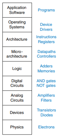
A system can be viewed from many levels of abstraction. Specifically in electronic computing systems we typically distinguish the following levels of abstraction:
In this course we focus on the levels of abstraction from digital circuits through computer architecture. When working on a level of abstraction it is always recommended to have knowledge of the levels just below and above. A computer scientist can not fully optimize code without understanding the architecture for which the program is written.
Discipline
Discipline is the act of intentionally restricting design choices such that one can work more productively at a higher level of abstraction. Using interchangeable parts is a familiar application of discipline. By limiting our choices to digital circuits we can easily combine components into sophisticated systems that ultimately outperform equivalent systems built using analog components in many applications.
The three Y’s
Additionally, designers use the three “y’s” to manage complexity:
- hierarchy: involves dividing a system into modules, then further subdividing each of these modules until the pieces are easy to understand.
- modularity: states that the modules have well-defined functions and interfaces, so that they connect together easily without unanticipated side effects.
- regularity: seeks uniformity among the modules. Common modules are reused many times, reducing the number of distinct modules that must be designed.
The Digital Abstraction
Most physical variables are continuous, especially in the realm of electrical engineering. Digital systems however represent information with discrete-valued variables, that is, variables with a finite number of distinct values.
The amount of information in a discrete valued variable with distinct states is measured in units of bits as
A binary variable conveys bit of information. Of course, the word bit is short for binary digit. A continuous signal theoretically contains an infinite amount of information because it can take on an infinite number of values. In practice however, noise and measurement errors limit the information to only 10 to 16 bits for most continuous signals.
Number Systems
In digital systems, binary or hexadecimal numbers are often more convenient than the base-10 number system.
Decimal Numbers
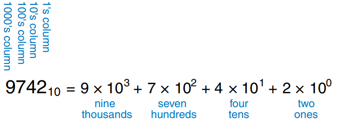
Decimal digits are joined together to form longer decimal numbers. Each column of a decimal number has ten times the weight of the previous column. From right to left, the column weight are 1, 10, 100, 1000 and so on. Decimal numbers are referred to as base 10. The base is indicated by a subscript after the number to prevent confusion when working in more than one base.
An -digit decimal number represents one of possibilities: . This is called the range of the number.
Binary Numbers
Bits represent one of two values, 0 or 1, and are joined together to form binary numbers. Each column of a binary number has twice the weight of the previous column, so binary numbers are base 2. In binary, the column weights are 1, 2, 3, 4, 16, 32, 64, 128 and so on.
An -bit binary number represents one of possibilities, .

Hexadecimal Numbers
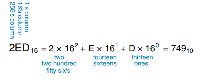
Writing long binary numbers becomes tedious and prone to error. A group of four bits represents one of possibilities. Hence, it is sometimes more convenient to work in base 16, called hexadecimal. Hexadecimal numbers use the digits 0 to 9 along with the letters A to F. Columns in base 16 have weights of and so on.
Bytes, Nibbles, Words
A group of eight bits is called a byte. It represents one of possibilities. A group of four bits, or half a byte, is called a nibble. It represents one of possibilities. One hexadecimal digit stores one nibble and two hexadecimal digits store one full byte.
Microprocessors handle data in chunks called words. The size of a word depends on the architecture of the microprocessor.
Within a group of bits, the bit in the 1’s column is called the least significant bit (lsb) and the bit at the other end is called the most significant bit (msb). Within a word, the bytes are identified as least significant byte (LSB) through most significant byte (MSB).
By coincidence, . Therefore the term kilo indicates . Similarly, mega (million) indicates and giga (billion) indicates .
1024 bytes is called a kilobyte (KB). 1024 bits is called a kilobit (Kb or Kbit). Similarly, MB, Mb, GB and Gb are used for millions and billions of bytes and bits. Memory capacity is usually measured in bytes. Communication speed is usually measured in bits/sec.
Binary Addition
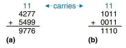
As in decimal addition, if the sum of two numbers is greater than what fits in a single digit, we carry a 1 into the next column. The bit that is carried over to the neighboring column is called the carry bit.
Digital systems usually operate on a fixed number of digits. Addition is said to overflow if the result is too big to fit in the available digits. overflow can be detected by checking for a carry out of the most significant column.
Signed Binary Numbers
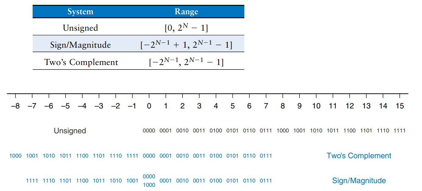
Sign/Magnitude Numbers
Sign/magnitude numbers are intuitively appealing because they match our custom of writing negative numbers with a minus sign followed by the magnitude. An -bit sign/magnitude number uses the most significant bit as the sign and the remaining bits as the magnitude (absolute value). A sign bit of 0 indicates positive and a sign bit of 1 indicates negative.
Unfortunately, ordinary binary addition does not work for sign/magnitude numbers. For example, using ordinary addition on gives , which is nonsense.
An -bit sign/magnitude number spans the range . Sign/magnitude numbers are slightly odd in that both and exist. Both indicate zero.
Two’s Complement Numbers
Two’s complement numbers are identical to unsigned binary numbers except that the most significant bit position has a weight of instead of . They overcome the shortcomings of sign/magnitude numbers: zero has a single representation, and ordinary addition works.
In two’s complement representation, zero is written as all zeros: . The most positive number has a 0 in the most significant position and 1’s elsewhere: . The most negative number has a 1 in the most significant position and o’s elsewhere: . -1 is written as all ones: .
The sign of a two’s complement number is reversed in a process called taking the two’s complement. The process consists of inverting all of the bits in the number, then adding 1 to the least significant bit position. This is useful to find the representation of a negative number or to determine the magnitude of a negative number.
Two’s complement numbers have the advantage that addition works properly for both positive and negative numbers. Recall that when adding -bit numbers, the carry out of the th bit is discarded.
Subtraction is performed by taking the two’s complement of the second number, then adding.
Unlike the sign/magnitude system, the two’s complement system has no separate -0.
In general, the range of an -bit two’s complement number spans . It should make sense that there is one more negative number than positive number because there is no -0.
The most negative number is sometimes called the weird number. Its two’s complement is found by inverting the bits (producing ) and adding 1, which produces , the weird number, again. Hence, this negative number has no positive counterpart.
Adding two -bit positive numbers or negative numbers may cause overflow if the result is greater than or less than . Adding a positive number to a negative number never causes overflow. Unlike signed numbers, a carry out of the most significant column does not indicate overflow. Instead, overflow occurs if the two numbers being added have the same sign bit and the result has the opposite sign bit.
When a two’s complement number is extended to more bits, the sign bit must be copied into the most significant bit positions. This process is called sign extension. For example the numbers 3 and -3 are written as 4-bit two’s complement numbers 0011 and 1101 respectively. They are sign-extended to seven bits by copying the sign bit into the three new upper bits to form 0000011 and 1111101 respectively.
Logic Gates
Logic gates are simple digital circuits that take one or more binary inputs and produce a binary output. Logic gates are drawn with a symbol showing the input (or inputs) and the output. Inputs are usually drawn to the left (or top) and outputs on the right (or bottom). Digital designers typically use letters near the beginning of the alphabet for gate inputs and the letter for the gate output. The relationship between the inputs and the output can be described with a truth table or a boolean equation. A truth table lists inputs on the left and the corresponding output on the right. It has one row for each possible combination of inputs. A Boolean equation is a mathematical expression using binary variables.
Gate
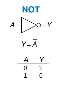
A gate has one input, , and one output, , as shown.
The gate’s output is the inverse of its input. If is , then is . If is , then is . This relationship is summarized by the truth table and boolean equation in the figure. This gate is also called an inverter.
Buffer
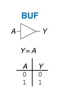
The other one-input logic gate is called a buffer as shown. From the logical point of view, a buffer is no different from a wire, so it might seem useless. However, from the analog point of view, the buffer might have desirable characteristics such as the ability to deliver large amounts of current to a motor, or the ability to quickly send its output to many gates. This is an example of why we need to consider multiple levels of abstraction to fully understand a system; the digital abstraction hides the real purpose of a buffer.
The triangle symbol indicates a buffer. A circle on the output is called a bubble and indicates inversion, as was seen in the gate symbol.
Gate
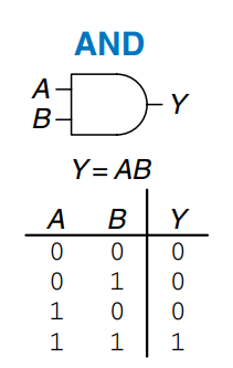
Two-input logic gates are more interesting. The gate as shown produces a output if and only if both and are . Otherwise, the output is . By convention, the inputs are listed in the order you would count up in binary.
The Boolean equation for an gate can be written in several ways: , or .
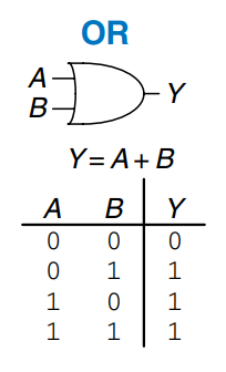
Gate
The gate as shown produces a output , if either or (or both) are .
The Boolean equation for an gate is written as or .
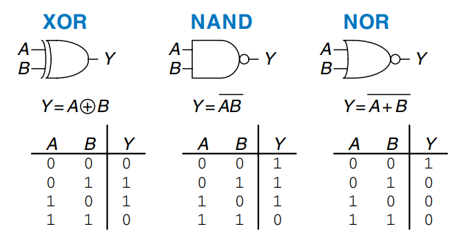
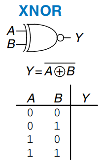
Other Two-Input Gates
Multiple-Input Gates
Many Boolean functions of three or more inputs exist. The most common are , , , , and . An -input gate produces a output when all inputs are . An -input gate produces a output when at least one input is . An -input gate is sometimes called a parity gate and produces a output if an odd number of inputs are .
Beneath the Digital Abstraction
A digital system uses discrete-valued variables. However, the variables are represented by continuous physical quantities such as the voltage on a wire, the position of a gear, or the level of fluid in a cylinder. hence, the designer must choose a way to relate the continuous variable to the discrete variable.
For example, consider representing a binary signal with a voltage on a wire. Let 0 volts (V) indicate and 5 V indicate . Any real system must tolerate some noise, so 4.97 V probably ought to be interpreted as as well. But what about 4.3 V? or 2.8 V?
Supply Voltage
Suppose the lowest voltage in the system is 0 V, also called ground or GND. The highest voltage in the system comes from the power supply and is usually called . In 1970’s and 1980’s technology, was generally 5 V. As chips have progressed to smaller transistors, has dropped to 3.3 V, 2.5 V, 1.8 V, 1.5 V, 1.2 V or even lower to save power and avoid overloading the transistors.
Logic Levels
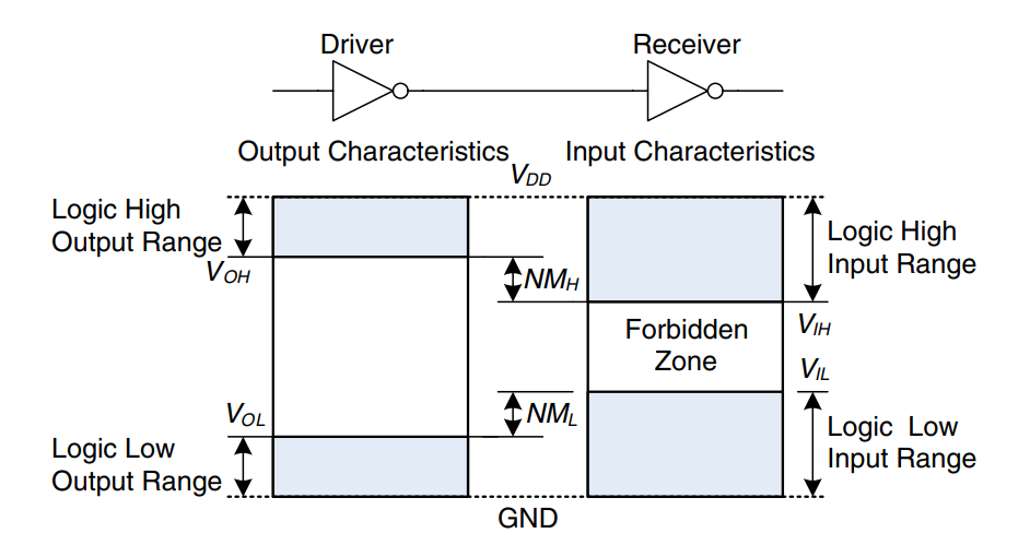
The mapping of a continuous variable onto a discrete binary variable is done by defining logic levels, as shown.
The first gate is called the driver and the second gate is called the receiver. The output of the driver is connected to the input of the receiver. The driver produces a (0) output in the range of 0 to or a (1) output in the range of to .
If the receiver gets an input in the range of 0 to , it will consider the input to be . If the receiver gets an input in the range of to , it will consider the input to be . If for some reason such as noise or faulty components, the receiver’s input should fall in the forbidden zone between and , the behavior of the gate is unpredictable. and are called the output and input high and low logic levels.
Noise Margins
Of course, the input and output levels must be chosen such that and , otherwise the input of the receiver can not possibly be interpreted in a correct way. Thus, even if the output of the driver is contaminated by some noise, the input of the receiver will still detect the correct logic level. The noise margin is the amount of noise that could be added to a worst-case output such that the signal can still be interpreted as a valid input:
DC Transfer Characteristics
The DC transfer characteristics of a gate describe the output voltage as a function of the input voltage when the input is changed slowly enough that the output can keep up. They are called transfer characteristics because they describe the relationship between input and output voltages.
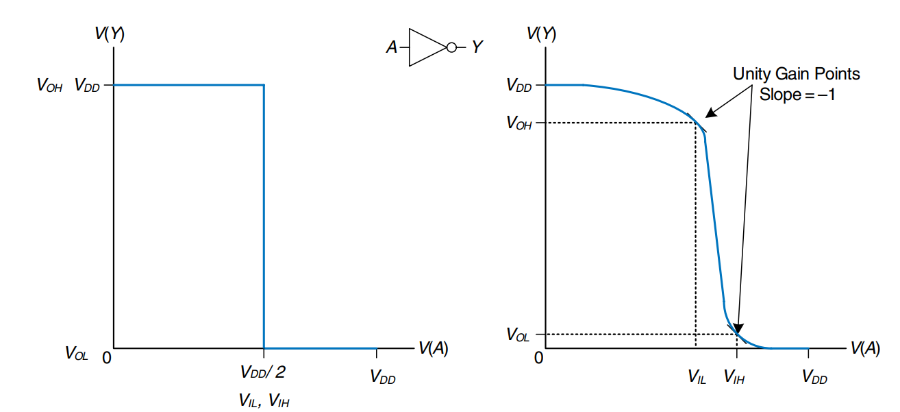
An ideal inverter would have an abrupt switching threshold at as shown on the left.
A real inverter changes more gradually between the extremes, as shown on the right. When the input voltage is 0, the output voltage . When , . However, the transition between these endpoints is smooth and may not be centered at exactly . This raises the question of how to define the logic levels.
A reasonable place to choose the logic levels is where the slope of the transfer characteristic is -1. These two points are called the unity gain points. Choosing logic levels at unity gain points usually maximizes the noise margins. If were reduced, would only increase by a small amount. But if were increased, would drop precipitously.
The Static Discipline
To avoid inputs falling into the forbidden zone, digital logic gates are designed to conform to the static discipline. The static discipline requires that, given logically valid inputs, every circuit element will produce logically valid outputs. By conforming to the static discipline, digital designers sacrifice the freedom of using arbitrary analog circuit elements in return for the simplicity and robustness of digital circuits. They raise the level of abstraction from analog to digital, increasing design productivity by hiding needless detail.
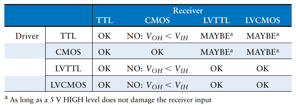
The choice of and logic levels is arbitrary, but all gates that communicate must have compatible logic levels. Therefore, gates are grouped into logic families such that all gates in a logic family obey the static discipline when used with other gates in the family.
Four major logic families that predominated from the 1970’s through the 1990’s are Transistor-Transistor Logic (TTL), Complementary Metal-Oxide-Semiconductor Logic (CMOS), Low Voltage TTL Logic (LVTTL), and Low Voltage CMOS Logic (LVCMOS). Since then, logic families have balkanized with a profliferation of even lower power supply voltages.

CMOS Transistors
Modern computers use transistors because they are reliable, small and cheap.. Transistors are electrically controlled switches that turn ON or OFF when a voltage or current is applied to a control terminal. The two main types of transistors are bipolar transistors and metal-oxide-semiconductor field effect transistors (MOSFETs).
MOSFETs are now the building blocks of almost all digital systems.
Semiconductors
MOSFETs are built from silicon, the predominant atom in rock and sand. Silicon (Si) is a group IV element, so it has four electrons in its valence shell and forms bonds with four adjacent atoms, resulting in a crystalline lattice.
By itself, silicone is a poor conductor because all the electrons are tied up in covalent bonds. However, it becomes a better conductor when small amounts of impurities, called dopant atoms, are carefully added. If a group V dopant such as arsenic (As) is added, the dopant atoms have an extra electron that is not involved in the bonds and can therefore move about the lattice freely, leaving an ionized dopant atom (As+) behind. The electron carries a negative charse, so we call arsenic an n-type dopant. On the other hand, if a group III dopant such as boron (B) is addedm the dopant atoms are missing an electron. This missing electron is called a hole. An electron from a neighboring silicon atom may mmove over to fill the missing bond, forming an ionized dopant atom (B-) and leaving a hole at the neighboring silicon atom. In a similar fashion, the hole can migrate around the lattice. The hole is a lack of negative charge, so it acts like a positively charged particle. Hence, we call boron a p-type dopant. Because the conductivity of silicon changes over many orders of magnitude depending on the concentration of dopants, silicon is called a semiconductor.
Diodes
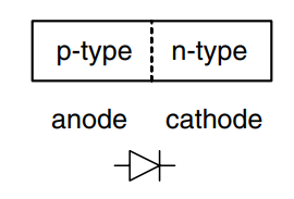
The junction between p-type and n-type silicon is called a diode. The p-type region is called the anode and the n-type region is called the cathode.
When the voltage on the anode rises above the voltage on the cathode, the diode is forward biased, and current flows through the diode from the anode to the cathode. But when the anode voltage is lower than the voltage on the cathode, the diode is reverse biased, and no current flows.

Capacitors
A capacitor consists of two conductors separated by an insulator. When a voltage is applied to one of the conductors, the conductor accumulates electric charge and the other conductor accumulates the opposite charge , The capacitance of the capacitor is the ratio of charge to voltage: . The capacitance is proportional to the size of the conductors and inversely proportional to the distance between them.
Capacitance is important, because charging or discharging a conductor takes time and energy. More capacitance means that a circuit will be slower and require more energy to operate.

nMOS and pMOS Transistors
A MOSFET is a sandwich of several layers of conducting and insulating materials. MOSFETs are built on thin flat wafers of silicon of about 15 to 30 cm in diameter. The manufacturing process begins with a bare wafer.The process involves a sequence of steps in which dopants are implanted into the silicon, thin films of silicon dioxide and silicon are grown, and metal is deposited. Between each step, the wafer is patterned so that the materials only appear where they are desired.
Because transistors are a fraction of a micron in length and the entire wafer is processed at once, it is inexpensive to manufacture billions of transistors at a time. Once processing is complete, the wafer is cut into rectangles called chips or dice that contain thousands, millions, or even billions of transistors. The chip is tested, then placed in a plastic or ceramic package with metal pins to connect it to a circuit board.
The MOSFET sandwich consists of a conducting layer called the gate on top of an insulating layer of silicone dioxide (SiO2) on top of the silicon wafer, called the substrate. Historically, the gate was constructed from metal, hence the name metal-oxide-semiconductor. modern manufacturing processes use polycrystalline silicon for the gate, because it does not melt during subsequent high-temperature processing steps. Silicon dioxide is better known as glass and is often simply called oxide in the semiconductor industry. The metal-oxide-semiconductor sandwich forms a capacitor, in which a thin layer of insulating oxide called a dielectric separates the metal and semiconductor plates.
There are two flavors of MOSFETs: nMOS and pMOS. The n-type transistors, called nMOS, have regions of n-type dopants adjacent to the gate called the source and the drain and are built on a p-type semiconductor substrate. The pMOS transistory are just the opposite, consisting of p-type source and drain regions in an n-type substrate.
A MOSFET behaves as a voltage-controlled switch in which the gate voltage creates an electric field that turns ON or OFF a connection between the source and drain. The term field effect transistor comes from this principle of operation.
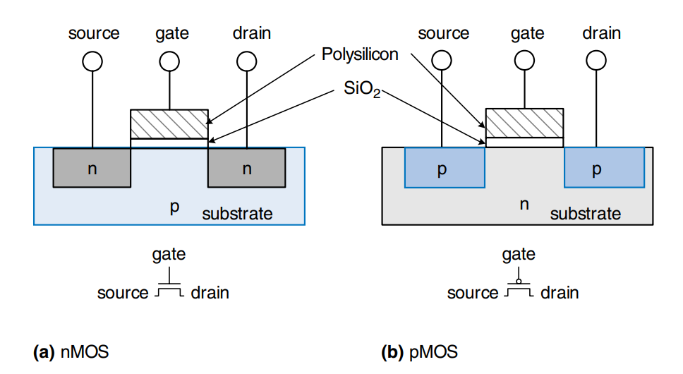
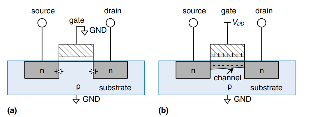
The substrate of an nMOS transistor is normally tied to GND. Consider the situation when the gate is also at 0 V, as shown. The diodes between the source or drain and the substrate are reverse biased because the source or drain voltage is nonnegative. Hence, there is no path for current to flow between the source and drain, so the transistor is OFF. Consider the situation when the gate is tied to . as shown. When a positive voltage is applied to the top plate of a capacitor, it establishes an electric field that attracts positive charge on the top plate and negative charge to the bottom plate. If the voltage is sufficiently large, so much negative charge is attracted to the underside of the gate that the region inverts from p-type to effectively become n-type. This inverted region is called the channel. Now the transistor has a continuous path from the n-type source through the n-type channel to the n-type drain, so electrons can flow from source to drain. The transistor is ON. The gate voltage required to turn on a transistor is called the threshold voltage, , and is typically 0.3 to 0.7 V.
pMOS transistors work just the opposite way. The substrate is tied to . When the gate is also at , the pMOS transistor is OFF. When the gate is at GND, the channel inverts to p-type and the pMOS transistor is ON.
However, MOSFETs are not perfect switches. nMOS transistors are excellent at passing 0’s, but very poor at passing 1’s. Specifically, when the gate of an nMOS transistor is at , the drain will only swing between 0 and . Similarily, pMOS transistory pass 1’s well, but 0’s poorly.
Considering both types of MOSFETs require both types of substrate, manufacturing processes typically start with a p-type wafer, then implant n-type regions called wells where the pMOS transistory will go. These processes that provide both flavors of transistors are called Complementary MOS, or CMOS. CMOS processes are used to build the vast majority of all transistors fabricated today.
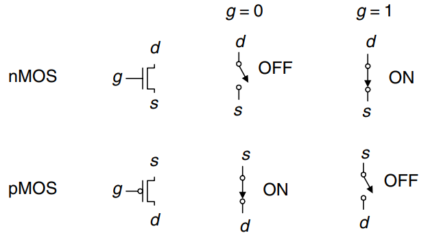
To summarize, CMOS processes give us two types of electrically controlled switches, as shown. The voltage at the gate (g) regulates the flow of current between the source (s) and drain (d). nMOS transistors are OFF when the gate is 0 and ON when the gate is 1. pMOS transistors are ON when the gate is 0 and OFF when the gate is 1.
CMOS Gate
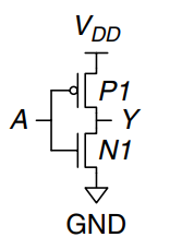
The triangle indicates GND, the flat bar indicates . The nMOS transistor, , is conneected between GND and the output. The pMOS transistor, , is connected between and the output. Both transistor gates are controlled by the input, .
If , is OFF and is ON. Hence, is connected to but not to GND, and is pulled up to a logic 1. passes a good 1. If , is ON and is OFF, and is pulled down to a logic 0. passes a good 0.
Other CMOS Logic Gates
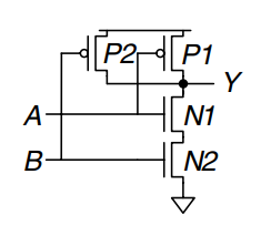
A two-input gate is displayed. In schematic diagrams, wires are always joined at three-way junctions. They are joined at four-way junctions only if a dot is shown. The nMOS transistors and are connected in series; both nMOS transistors must be ON to pull the output down to GND. The pMOS transistors and are in parallel; only one pMOS transistor must be ON to pull the output up to .
The figure shows a general form to construct any inverting logic gate, such as , or . nMOS transistors are good at passing 0’s, so a pull-down network of nMOS transistors is places between the output and GND to pull the output down to 0. pMOS transistors are good at passing 1’s, so a pull-up network of pMOS transistors is placed between the output and to pull the output up to 1. The networks may consist of transistors in series or in parallel. When transistors are in parallel, the network is ON if either transistor is ON. When transistors are in series, the network is ON only if both transistors are ON. The slash across the input wire indicates that the gate may receive multiple inputs.
If both the pull-up and pull-down networks were ON simultaneously, a short circuit would exists between and GND. The output of the gate might be in the forbidden zone and the transistors would consume large amounts of power, possibly enough to burn out. On the other hand, if both the pull-up and pull-down networks were OFF simultaneously, the output would be connected to neither nor GND. We say that the output floats. Its value is again undefined. Floating outputs are usually undesirable, but in some cases they can be used to the designer’s advantage.
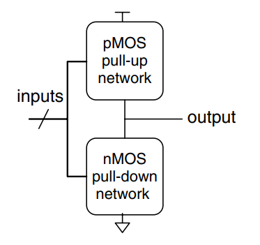
In a properly functioning logic gate, one of the networks should be ON and the other OFF at any given time, so that the output is pulled HIGH or LOW but never shorted or floating. We can guarantee this by using the rule of conduction complements. When nMOS transistors are in series, the pMOS transistors must be in parallel. When nMOS transistors are in parallel, the pMOS transistors must be in series.
Transmission Gates
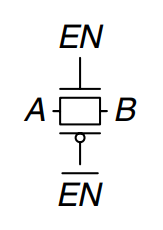
Recall that nMOS transistors are good at passing 0 and pMOS transistors are good at passing 1, so the parallel combination of the two passes both values well. This is what’s called a transmission gate or pass gate. The control signals are called enables, and .
Pseudo-nMOS Logic
An -input CMOS gate uses nMOS transistors in parallel and pMOS transistors in series. Transistors in series are slower than transistors in parallel, just as resistors in series have more resistance than resistors in parallel. Moreover, pMOS transistors are slower than nMOS transistors because holes cannot move around the silicon lattice as fast as electrons. Therefore the parallel nMOS transistors are fast and the series pMOS transistors are slow.
Pseudo-nMOS logic replaces the slow stack of pMOS transistors with a single weak pMOS transistor that is always ON, as shown. This pMOS transistor is often called a weak pull-up. The physical dimensions of the pMOS transistor are selected so that the pMOS transistor will pull the output, , HIGH weakly - that is, only if none of the nMOS transistors are ON. But if any nMOS transistor is ON, it overpowers the weak pull-up and pulls down close enough to GND to produce a logic 0.
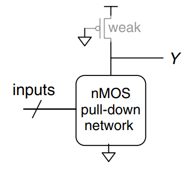
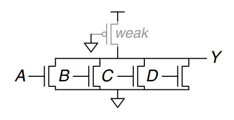
The advantage of pseudo-nMOS logic is that it can be used to build fast gates with many inputs. For example, as shown, a pseudo-nMOS four-input gate. Pseudo-nMOS gates are useful for certain memory and logic arrays discussed later. The disadvantage is that a short circuit exists between and GND when the output is LOW; the weak pMOS and nMOS transistors are both ON. The short circuit draws continuous power, so pseudo-nMOS logic must be used sparingly.
Power Consumption
Power consumption is the amount of energy used per unit time. Digital systems draw both dynamic and static power. Dynamic power is the power used to charge capacitance as signals change between 0 and 1. Static power is the power used even when signals do not change and the system is idle.
Logic gates and the wires that connect them have capacitance. The energy drawn from the power supply to charge a capacitance to voltage is . If the voltage on the capacitor switches at frequency , it charges the capacitor times and discharges it times per second. Discharging does not draw energy from the power supply, so the dynamic power consumption is
Electrical systems draw some current even when they are idle. When transistors are OFF, they leak a small amount of current. Some circuits, such as the pseudo-nMOS gate, have a path from to GND through which current flows continuously. The total static current, , is also called the leakage current or the quiescent supply current flowing between and GND. The static power consumption is proportional to this static current: