Digital Building Blocks
- Digital Building Blocks
- Arithmetic Circuits
- Number Systems
- Sequential Building Blocks
- Memory Arrays
- Logic Arrays
Digital Building Blocks
Arithmetic Circuits
Arithmetic circuits are the central building blocks of computers. Computers and digital logic perform many arithmetic functions: addition, subtraction, comparison, shift, multiplication and division.
Addition
Addition is one of the most common operations in digital systems. We first consider how to add two 1-bit binary numbers. We then extend to -bit binary numbers. Adders also illustrate trade-offs between speed and complexity.
Half Adder
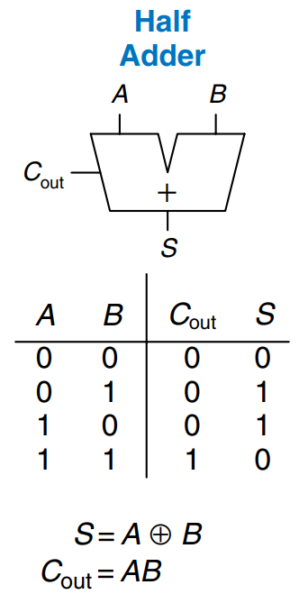
We begin by building a 1-bit half adder. As shown in the figure, the half adder has two inputs, and , and two outputs, and . is the sum of and . If and are both 1, is 2, which cannot be represented with a single binary digit. Instead, it is indicated with a carry out, , in the next column. The half adder can be built from an gate and an gate.
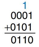
In a multi-bit adder, is added or carried in to the next most significant bit. For example, as shown in the figure, the carry bit shown in blue is the output, , of the first column of 1-bit addition and the input, , to the second column of addition. However, the half adder lacks a input to accept of the previous column. The full adder, described in the next section, solves this problem.
Full Adder
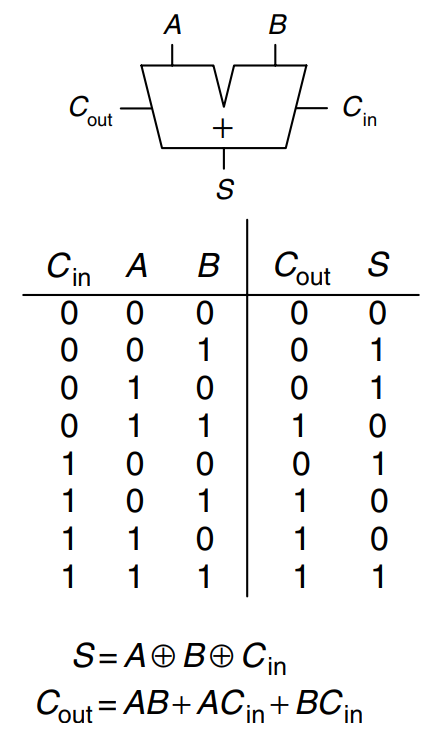
A full adder accepts the carry in, as shown. The figure also shows the output equations for and .
Carry Propagate Adder
An -bit adder sums two -bit inputs, and , and a carry in, , to produce an -bit result, , and a carry out, . It is commonly called a carry propagate adder (CPA) because the carry out of one bit propagates into the next bit. The symbol for a CPA is shown in the figure; it is drawn just like a full adder except that , , and are busses rather than single bits. Three common CPA implementations are called ripple-carry adders, carry-lookahead adders, and prefix adders.
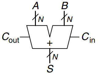
Ripple-Carry Adder
The simplest way to build an -bit carry propagate adder is to chain together full adders. The of one stage acts as the of the next stage, as shown in the figure for 32-bit addition. This is called a ripple-carry adder. It is a good application of modularity and regularity: the full adder module is reused many times to form a larger system. The ripple-carry adder has the disadvantage of being slow when is large. depends on , which depends on and so forth all the way back to , as shown blue in the figure. We say that the carry ripples through the carry chain. The delay of the adder, , grows directly with the number of bits, as given by below equation, where is the delay of a full adder.

Carry-Lookahead Adder
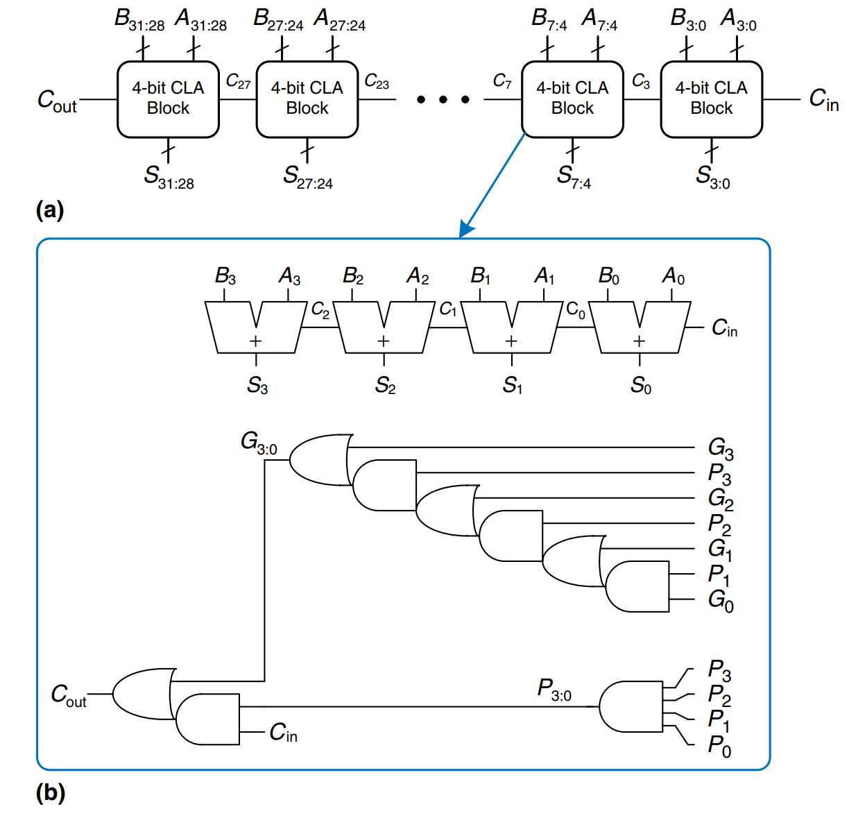
The fundamental reason that large ripple-carry adders are slow is that the carry signals must propagate through every bit in the adder. A carry-lookahead adder is another type of carry propagate adder that solves this problem by dividing the adder into blocks and providing circuitry to quickly determine the carry out of a block as soon as the carry in is known. This it is said to look ahead across the blocks rather than waiting to ripple through all the full adders inside a block, For example, a 32-bit adder may be divided into eight 4-bit blocks.
Carry-lookahead adders use generate () and propagate () signals that describe how a column or block determines the carry out. The -th column of an adder is said to generate a carry if it produces a carry out independent of the carry in. The -th column of an adder is guaranteed to generate a carry, , if and are both 1. Hence , the generate signal for column , is calculated as . The column is said to propagate a carry if it produces a carry out whenever there is a carry in. The -th column will propagate a carry in, , if either or is 1. Thus, . Using these definitions, we can rewrite the carry logic for a particular column of the adder. The -th column of an adder will generate a carry out, , if it either generates a carry, , or propagates a carry in, . In equation form:
The generate and propagate definitions extend to multiple-bit blocks. A block is said to generate a carry if it produces a carry out independent of the carry in to the block. The block is said to propagate a carry if it produces a carry out whenever there is a carry in to the block. We define and as generate and propagate signals for blocks spanning columns through .
A block generates a carry if the most significant column generates a carry, or if the most significant column propagates a carry and the previous column generated a carry, and so forth. For example, the generate logic for a block spanning columns 3 through 0 is
A block propagates a carry if all the columns in the block propagate the carry. For example, the propagate logic for a block spanning columns 3 through 0 is
Using the block generate and propagate signals, we can quickly compute the carry out of the block, , using the carry in to the block, .
Figure a) shows a 32-bit carry-lookahead adder composed of eight 4-bit blocks. Each block contains a 4-bit ripple-carry adder and some lookahead logic to compute the carry out of the block given the carry in, as shown in figure b). The and gates beeded to compute the single-bit generate and propagate signals, and , are left out for brevity. Again, the carry-lookahead adder demonstrates modularity and regularity.
All of the CLA blocks compute the single-bit and block generate and propagate signals simultaneously. The critical path starts with computing and in the first CLA block. then advances directly to through the gate in each block until the last. For a large adder, this is much faster than waiting for the carries to ripple through each consecutive bit of the adder. Finally, the critical path through the last block contains a short ripple-carry adder. Thus, an -bit adder divided into -bit blocks has a delay
where is the delay of the individual generate/propagate gates (a single or gate) to generate and , is the delay to find the generate/propagate signals and for a -bit block, and is the delay from to through the logic of the -bit CLA block. For , the carry-lookahead adder is generally much faster than the ripple-carry adder. However, the adder delay still increases linearly with .
Prefix Adder
Prefix adders extend the generate and propagate logic of the carry-lookahead adder to perform addition even faster. They first compute and for pairs of columns, then for blocks of 4, then for blocks of 8, then 16, and so forth until the generate signal for every column is known. The sums are computed from these generate signals.
In other word, the strategy of a prefix adder is to compute the carry in, , for each column, , as quickly as possible, then to compute the sum using
Define column to hold , so and . Then because there will be a carry out of column if the block spanning columns through generates a carry. The generated carry is either generated in column -1 or generated in a previous column and propagated. Thus, we can rewrite above equation as
Hence, the main challenge is to rapidly compute all the block generate signals , , ,…, . These signals, along with are called prefixes.
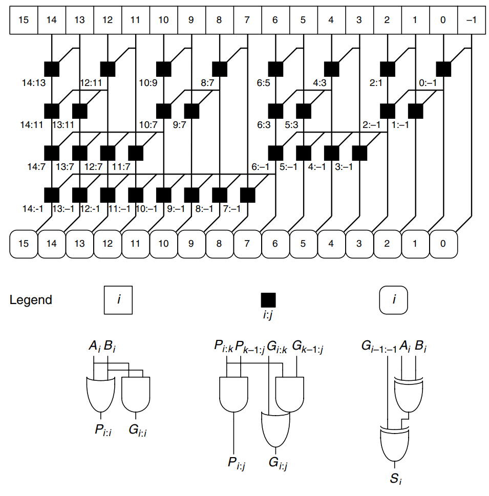
The figure shows an -bit prefix adder. The adder begins with a precomputation to form and for each column from and using and gates. It then uses levels of black cells to form the prefixes of and . A black cell takes inputs from the upper part of a block spanning bits and from the lower part of a block spanning bits . It combines these parts to form generate and propagate signals for the entire block spanning bits using the following equations:
In other words, a block spanning bits will generate a carry if the upper part generates a carry or if the upper part propagates a carry generated in the lower part. The block will propagate a carry if both the upper and lower parts propagate the carry. Finally, the prefix adder computes the sums using the equations for above.
In summary, the prefix adder achieves a delay that grows logarithmically rather than linearly with the number of columns in the adder. This speedup is significant, especially for adders with 32 or more bits, but it comes at the expense of more hardware than a simple carry-lookahead adder. The network of black cells is called a prefix tree.
The general principle of using prefix trees to perform computations in time that grows logarithmically with the number of inputs is a powerful technique. With some cleverness, it can be applied to many other types of circuits.
The critical path for an -bit prefix adder involves the precomputation of and followed by stages of black prefix cells to obtain all the prefixes. then proceeds through the final gate at the bottom to compute . Mathematically, the delay of an -bit prefix adder is
where is the delay of a black prefix cell.
Hardware description languages provide the operation to specify a CPA. Modern synthesis tools select among many possible implementations, choosing the cheapest (smallest) design that meets the speed requirements. This greatly simmplifies the designer’s job. The example describes a CPA with carries in and out.
module adder #(parameter N = 8)
              (input  [N-1:0] a, b,
               input          cin,
               output [N-1:0] s,
               output         cout);
  assign {cout, s} = a + b + cin;
endmodule

Subtraction
Adders can add positive and negative numbers using two’s complement number representation. Subtraction is almost as easy: flip the sign of the second number, then add. Flipping the sign of a two’s complement number is done by inverting the bits and adding 1.
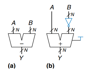
To compute , first create the two’s complement of : Invert the bits of to obtain and add 1 to get . Add this quantity to to get . This sum can be performed with a single CPA by adding with . The figure shows the symbol for a subtractor and the underlying hardware for performing .
This example describes a subtractor.
module subtractor #(parameter N = 8)
                   (input  [N-1:0] a, b,
                    output [N-1:0] y);
  assign y = a - b;
endmodule

Comparators
A comparator determines whether two binary numbers are equal or if one is greater or less than the other. A comparator receives two -bit binary numbers, and . There are two common types of comparators.
An equality comparator produces a single output indicating whether is equal to (). A magnitude comparator produces one or more outputs indicating the relative values of and .
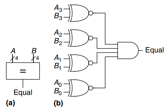
The equality comparator is the simpler piece of hardware. The figure shows the symbol and implementation of a 4-bit equality comparator. It first checks to determine whether the corresponding bits in each column of and are equal, using gates. The numbers are equal if all of the columns are equal.
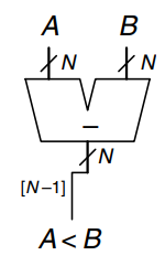
Magnitude comparison is usually done by computing and looking at the sign (most significant bit) of the result, as shown. If the result is negative (i.e., the sign bit is 1), then is less than . Otherwise is greater or equal to .
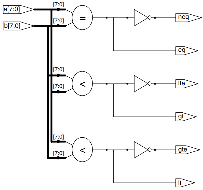
The example shows how to use various comparison operations.
module comparators # (parameter N = 8)
                     (input  [N-1:0] a, b,
                      output         eq, neq,
                      output         lt, lte,
                      output         gt, gte);
  assign eq = (a == b);
  assign neq = (a != b);
  assign lt = (a < b);
  assign lte = (a <= b);
  assign gt = (a > b);
  assign gte = (a >= b);
endmodule
ALU
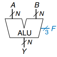
An Arithmetic/Logical Unit (ALU) combines a variety of mathematical and logical operations into a single unit. For example, a typical ALU might perform addition, subtraction, magnitude comparison, and operations. The ALU forms the heart of most computer systems.
The figure shows the symbol for an -bit ALU with -bit inputs and outputs. The ALU receives a control signal, , that specifies which function to perform. Control signals will generally be shown in blue to distinguish them from the data. The table lists typical functions that the ALU can perform.
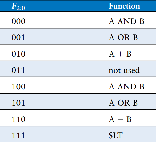
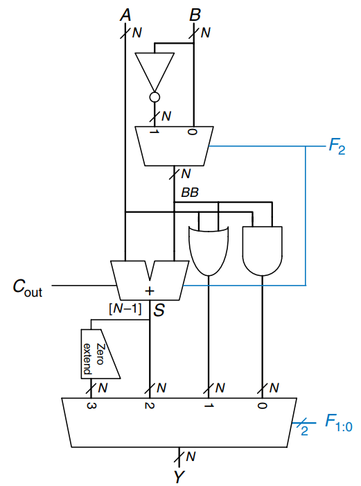
The figure shows an implementation of the ALU. The ALU contains an -bit adder and two-input and gates. It also contains an inverter and a multiplexer to optionally invert input when the control signal is asserted. A 4:1 multiplexer chooses the desired function based on the control signals. More specifically, the arithmetic and logical blocks in the ALU operate on and . is either or , depending on . If , the output multiplexer chooses . If , the ALU computes . If , the ALU performs addition or subtraction. Note that is also the carry in to the adder. Also remember that in two’s complement arithmetic. If , the ALU computes . If the ALU computes .
When , the ALU performs the set if less than (SLT) operation. When , . Otherwise, . In other words, is set to 1 if is less than .
SLT is performed by computing . If is negative, . The zero extend unit produces an -bit output by concatenating its 1-bit input with 0’s in the most significant bits. The sign bit of is their input to the zero extend unit.
Some ALUs produce extra outputs, called flags, that indicate information about the ALU output. For example, an overflow flag indicates that the result of the adder overflowed. A zero flag indicates that the ALU output is 0.
Shifters and Rotators
Shifters and rotators move bits and multiply or divide by powers of 2. As the name implies, a shifter shifts a binary number left or right by a specified number of positions. There are several kinds of commonly used shifters:
- Logical shifter - shifts the number to the left (LSL) or right (LSR) and fills empty spots with 0’s.
- Ex: 11001 LSR 2 = 00110; 11001 LSL 2 = 00100
- Arithmetic shifter - is the same as a logical shifter, but on right shifts fills the most significant bits with a copy of the old most significant bit. This is useful for multiplying and dividing signed numbers. Arithmetic shift left (ASL) is the same as logical shift left (LSL).
- Ex: 11001 ASR 2 = 11110; 11001 ASL 2 = 00100
- Rotator - rotates number in circle such that empty spots are fulled with bits shifted off the other end.
- Ex: 11001 ROR 2 = 01110; 11001 ROL 2 = 00111
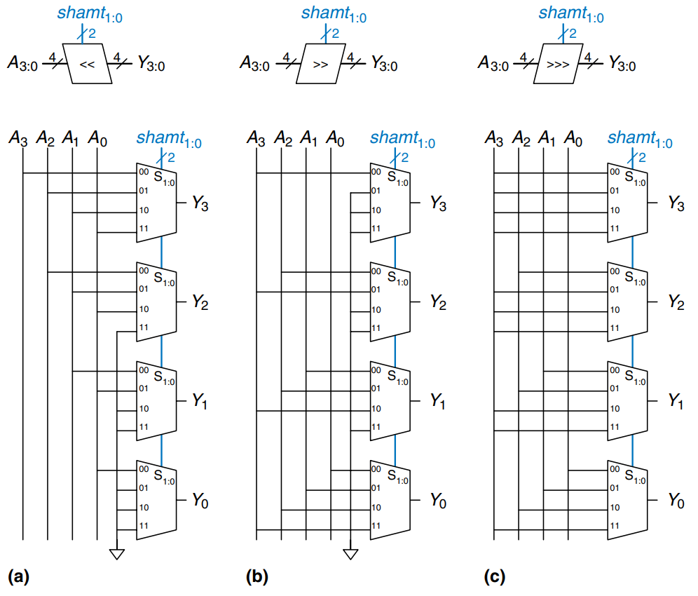
An -bit shifter can be built from :1 multiplexers. The input is shifted by 0 to bits, depending on the value of the -bit select lines. The figure shows the symbol and hardware of 4-bit shifters. The operators , , and typically indicate shift left (a)), logical shift right (b)), and arithmetic shift right (c)), respectively. Depending on the value of the 2-bit shift amount, , the output, , receives the input, , shifted by 0 to 3 bits. For all shifters, when , .
A left shift is a special case of multiplication. A left shift by bits multiplies the number by . For example, is equivalent to .
An arithmetic right shift is a special case of division. An arithmetic right shift by bits divides the number by . For example, is equivalent to .
Multiplication
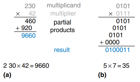
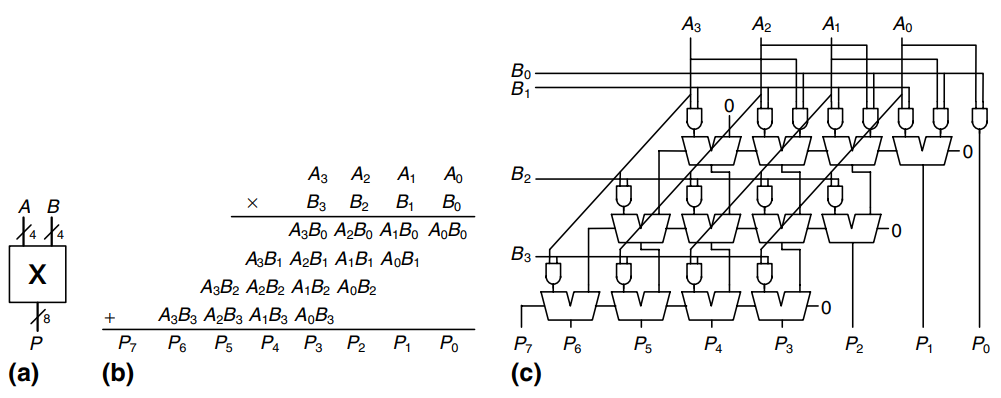
Multiplication of unsigned binary numbers is similar to decimal multiplication but involves only 1’s and 0’s. The figure compares multiplication in decimal and binary. In both cases, partial products are formed by multiplying a single digit of the multiplies with the entire multiplicand. The shifted partial products are summed to form the result.
In general, an multiplies multiplies two -bit numbers and produces a -bit result. The partial products in binary multiplication are either the multiplicand or all 0’s. Multiplication of 1-bit binary numbers is equivalent to the operation, so gates are used to form the partial products.
The figure shows the symbol, function and implementation of a multiplier. The multiplier receives the multiplicand and multiplier, and , and produces the product, . Each partial product is a single multiplier bit (, , or ) the multiplicand bits (). With -bit operands, there are partial products and stages of 1-bit adders. For example, for a multiplier, the partial product of the first row is . This partial product is added to the shifted second partial product, . Subsequent rows of gates and adders form and add the remaining partial products.
As with adders, many different multiplier designs with different speed/cost trade-offs exist. Synthesis tools may pick the most appropriate design given the timing constraints.
module multiplier # (parameter N = 8)
                    (input  [N-1:0]   a, b,
                     output [2*N-1:0] y);
  assign y = a * b;
endmodule

Division
Binary division can be performed using the following algorithm for normalized unsigned numbers in the range :
R = A
for i = N - 1 to 0
	D = R - B
	if D < 0 then Q_i = 0, R' = R
	else          Q_i = 1, R' = D
	if i != 0 then R = 2*R'
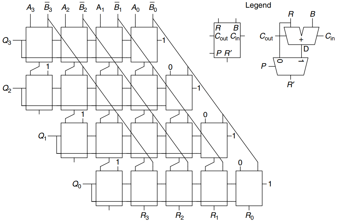
The partial remainder, , is initialized to the dividend, . The divisor, , is repeatedly subtracted from this partial remainder to determine whether it fits. If the difference, , is negative, then the quotient bit, , is 0 and the difference is discarded. Otherwise, is 1, and the partial remainder is updated to be the difference. In any event, the partial remainder is then doubled, and the process repeats. The result satisfies:
The figure shows a schematic of a 4-bit array divider. The divider computes and produces a quotient, , and a remainder, . The legend shows the symbol and schematic for each block in the array divider. The signal indicates whether is negative. It is obtained from the output of the leftmost block in the row, which is the sign of the difference.
The delay of an -bit array divider increases proportionally to because the carry must ripple through all stages in a row before the sign is determined and the multiplexer selects or . This repeats for all rows. Division is a slow and expensive operation in hardware and theerefore should be used as infrequently as possible.
Number Systems
Computers operate on both integers and fractions. So far, we have only considered representing signed or unsigned integers. This section introduces fixed- and floating point number systems that can also represent rational numbers. Fixed-point numbers are analogous to decimals; some of the bits represent the integer part, and the rest represent the fraction. Floating-point numbers are analogous to scientific notation, with a mantissa and an exponent.
Fixed-Point Number Systems
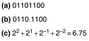
Fixed-point notation has an implied binary point between the integer and fraction bits, analogous to the decimal point between the integer and fraction digits of an ordinary decimal number. The figure a) shows a fixed-point number with four integer bits and four fraction bits. b) shows the implied binary point in blue, and c) shows the equivalent decimal value.
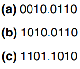
Signed fixed-point numbers can use either two’s complement (c)) or sign/magnitude (b)) notations. The figure shows the fixed-point representation of -2.375 using both notations with four integer and four fraction bits. The implicit binary point is shown in blue for clarity. In sign/magnitude form, the most significant bit is used to indicate the sign. The two’s complement representation is formed by inverting the bits of the absolute value (a)) and adding a 1 to the least significant /rightmost) bit. In this case, the least significant bit position is the column.
Like all binary number representations, fixed-point numbers are just a collection of bits. There is no way of knowing the existence of the binary point except through agreement of those people interpreting the number.
Floating-Point Number Systems
Floating-point numbers are analogous to scientific notation. They circumvent the limitation of having a constant number of integer and fractional bits, allowing the representation of very large and very small numbers. Like scientific notation, floating-point numbers have a sign, mantissa (M), base (B), and exponent (E), as shown. For example. the number is the decimal scientific notation for 4100. It has a mantissa of 4.1, a base of 10, and an exponent of 3. The decimal point floats to the position right after the most significant digit. Floating-point numbers are base 2 with a binary mantissa. 32 bits are used to represent 1 sign bit, 8 exponent bits, and 23 mantissa bits.

In binary floating-point, the first bit of the mantissa (to the left of the binary point) is always 1 and therefore need not be stored. It is called the implicant leading one. The figure shows the modified floating point representation of . The implicit leading one is not included in the 23-bit mantissa for efficiency. Only the fraction bits are stored. This frees up an extra bit for useful data.

We make one final modification to the exponent field. The exponent needs to represent both positive and negative exponents. To do so, floating-point uses a biased exponent, which is the original exponent plus a constant bias. 32-bit floating-point uses a bias of 127. For example, for the exponent 7, the biased exponent is . For the exponent -4, the biased exponent is . The figure shows represented in floating-point notation with an implicit leading one and a biased exponent of 134. This notation conforms to the IEEE 754 floating-point standard.
Special Cases: 0, , and NaN
The IEEE floating-point standard has special cases to represent numbers such as zero, infinity, and illegal results. For example, representing the number zero is problematic in floating-point notation because of the implicit leading one. Special codes with exponents of all 0’s or all 1’s are reserved for these special cases. The table shows the floating-point representations of 0, , and NaN. As with sign/magnitude numbers, floating-point has both positive and negative 0. NaN is used for numbers that don’t exist, such as or .

Single- and Double-Precision Formats
So far, we have examined 32-bit floating-point numbers. This format is also called single-precision, single, or float. The IEEE 754 standard also defines 64-bit double-precision (also called double) numbers that provide greater precision and greater range. The table shows the number of bits used for the fields in each format.
Excluding the special cases mentioned earlier, normal single-precision numbers span a range of to . They have a precision of about seven significant decimal digits (because ). Similarly, normal double-precision numbers span a range of to and have a precision of about 15 significant decimal digits.

Rounding
Arithmetic results that fall outside of the available precision must round to a neighboring number. The rounding modes are (1) round down, (2) round up, (3) round toward zero, and (4) round to nearest. The default rounding mode is round to nearest. In the round to nearest mode, if two numbers are equally near, the one with a 0 in the least significant position of the fraction is chosen.
Recall that a number overflows when its magnitude is too large to be represented. Likewise, a number underflows when it is too tiny to be represented. In round to nearest mode, overflows are rounded up to and underflows are rounded down to 0.
Floating-Point Addition
Addition with floating-point numbers is not as simple as addition with two’s complement numbers. The steps for adding floating-point numbers with the same sign are as follows:
- Extract exponent and fraction bits
- Prepend leading 1 to form the mantissa
- Compare exponents
- Shift smaller mantissa if necessary
- Add mantissas
- Normalize mantissa and adjust exponent if necessary
- Round result
- Assemble exponent and fraction back into floating-point number
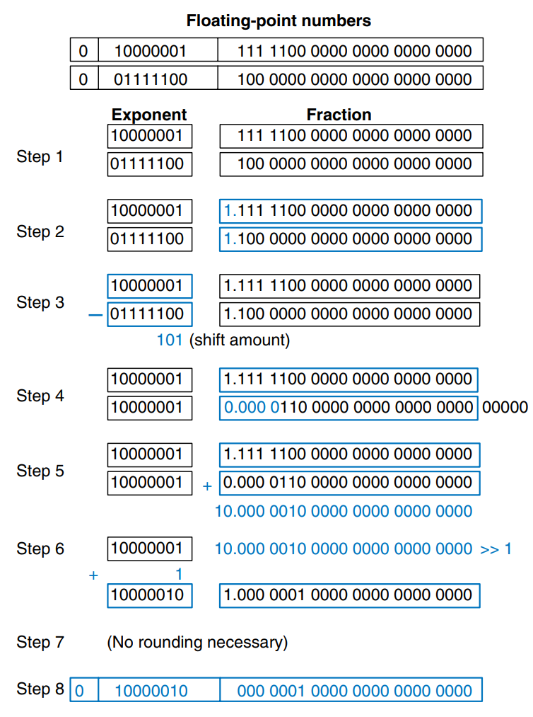
The figure show the floating-point addition of 7.875 () and 0.1875 (). The result is 8.0625 (). After the fraction and exponent bits are extracted and the implicit leading 1 is prepended in steps 1 and 2, the exponents are compared by subtracting the smaller exponent from the larger exponent. The result is the number of bits by which the smaller number is shifted to the right to align the implied binary point (i.e. to make the exponents equal) in step 4. The aligned numbers are added. Because the sum has a mantissa that is greater than or equal to 2.0, the result is normalized by shifting it to the right by one bit and incrementing the exponent. In this example, the result is exact, so no rounding is necessary. The result is stored in floating-point notation by removing the implicit leading one of the mantissa and prepending the sign bit.
Floating-point arithmetic is usually done in hardware to make it fast. This hardware, called the floating-point unit (FPU) is typically distinct from the central processing unit (CPU). The infamous floating-point division (FDIV) bug in the Pentium FPU cost Intel 475 million dollars to recall and replace defective chips. The bug occurred simply because a lookup table was not loaded correctly.
Sequential Building Blocks
Counters
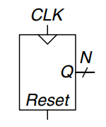
An -bit binary counter, as shown, is a sequential arithmetic circuit with clock and reset inputs and an -bit output, . Reset initializes the output to 0. The counter then advances through all possible outputs in binary order, incrementing on the rising edge of the clock.
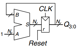
The figure shows an -bit counter composed of an adder and a resettable register. On each cycle, the counter adds 1 to the value stored in the register.
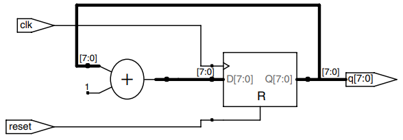
The example describes a binary counter with asynchronous reset.
module counter # (parameter N = 8)
                 (input              clk,
                  input              reset,
                  output reg [N-1:0] q);
  always @ (posedge clk or posedge reset)
    if (reset) q <= 0;
    else q <= q + 1;
endmodule
Shift Registers
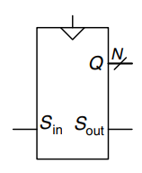
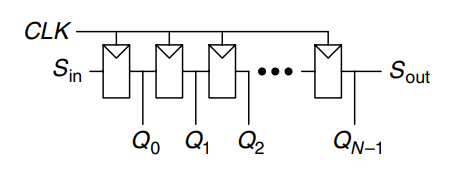
A shift register has a clock, a serial input, , a serial output, , and parallel outputs, , as shown. On each rising edge of the clock, a new bit is shifted in from and all the subsequent contents are shifted forward. The last bit in the shift register is available at . Shift registers can be viewed as serial-to-parallel converters. The input is provided serially at . After cycles, the past inputs are available in parallel at .
A shift register can be constructed from flip-flops connected in series, as shown. Some shift registers also have a reset signal to initialize all of the flip-flops.
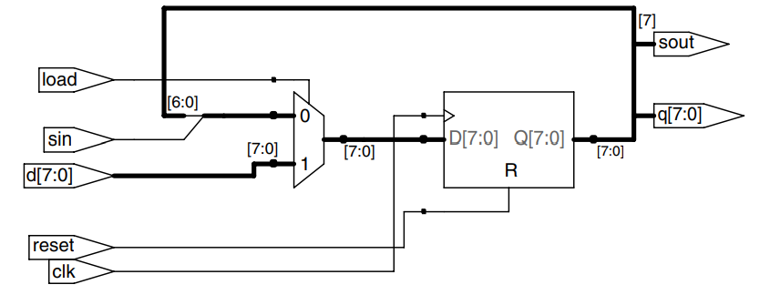
A related circuit is a parallel-to-serial converter that loads bits in parallel, then shifts them out one at a time. A shift register can be modified to perform both serial-to-parallel and parallel-to-serial operations by adding a parallel input, , and a control signal, , as shown. When is asserted, the flip-flops are loaded in parallel from the inputs. Otherwise, the shift register shifts normally.

The example describes such a circuit.
module shiftreg # (parameter N = 8)
                  (input              clk,
                   input              reset, load,
                   input              sin,
                   input      [N-1:0] d,
                   output reg [N-1:0] q,
                   output             sout);
  always @ (posedge clk or posedge reset)
    if (reset) q <= 0;
    else if (load) q <= d;
    else q <= {q[N-2:0], sin};

  assign sout = q[N-1]
endmodule
Scan Chains
Shift registers are often used to test sequential circuits using a technique called scan chains. Testing combinational circuits is relatively straightforward. Known inputs called test vectors are applied, and the outputs are checked against the expected result. Testing sequential circuits is more difficult, because the circuits have state. Starting from a known initial condition, a large number of cycles of test vectors may be needed to put the circuit into a desired state. For example, testing that the most significant bit of a 32-bit counter advances from 0 to 1 require resetting the counter, then applying clock pulses.
To solve this problem, designers like to be able to directly observe and control all the state of the machine. This is done by adding a test mode in which the contents of all flip-flops can be read out or loaded with desired values. Most systems have too many flip-flops to dedicate individual pins to read and write each flip-flop. Instead, all the flip-flops in the system are connected together into a shift register called a scan chain. In normal operation, the flip-flops load data from their input and ignore the scan chain. In test mode, the flip-flops serially shift their contents out and shift in new contents using and . The load multiplexer is usually integrated into the flip-flop to produce a scannable flip-flop. The figure shows the schematic and symbol for a scannable flip-flop and illustrates how the flops are cascaded to build an -bit scannable register.
For example, the 32-bit counter could be tested by shifting in the pattern 01111….111 in test mode, counting for one cycle in normal mode, then shifting out the result, which should be 10000…000. This requires only 32 + 1 + 32 = 65 cycles.

Memory Arrays
The previous sections introduced arithmetic and sequential circuits for manipulating data. Digital systems also require memories to store the data used and generated by such circuits. Registers built from flip-flops are a kind of memory that stores small amounts of data. This section describes memory arrays that can efficiently store large amounts of data.
Overview
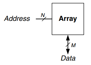
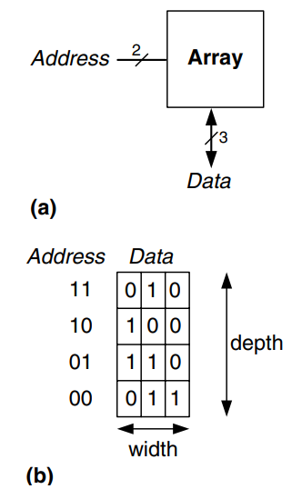
The figure shows a generic symbol for a memory array. The memory is organized as a two-dimensional array of memory cells. The memory reads or writes the contents of one of the rows of the array. This row is specified by an Address. The value read or written is called Data. An array with -bit addresses and -bit data has rows and columns. Each row of data is called a word. Thus, the array contains -bit words.
The figure shows a memory array with two address bits and three data bits. The two address bits specify one of the four rows (data words) in the array. Each data word is three bits wide. b) shows some possible contents of the memory array.
The depth of an array is the number of rows, and the width is the number of columns, also called the word size. The size of an array is given as depth width. The figure is a 4-word 3-bit array, or simply a array.
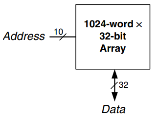
The symbol for a 1024-word 32-bit array is shown in the figure.
Bit Cells
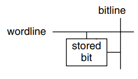
Memory arrays are built as an array of bit cells, each of which stores 1 bit of data. The figure shows that each bit cell is connected to a wordline and a bitline. For each combination of address bits, the memory asserts a single wordline that activates the bit cells in that row. When the wordline is HIGH, the stored bit transfers to or from the bitline. Otherwise, the bitline is disconnected from the bit cell. The circuitry to store the bit varies with memory type.
To read a bit cell, the bitline is initially left floating (Z). Then the wordline is turned ON, allowing the stored value to drive the bitline to 0 or 1. To write a bit cell, the bitline is strongly driven to the desired value. Then the wordline is turned ON, connecting the bitline to the stored bit. The strongly driven bitline overpowers the contents of the bit cell, writing the desired value into the stored bit.
Organization
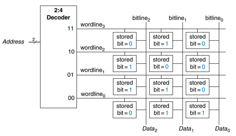
The figure shows the internal organization of a 4 3 memory array. Of course, practical memories are much larger, but the behavior of larger array can be extrapolated from the smaller array.
During a memory read, a wordline is asserted and the corresponding row of bit cells drives the bitlines HIGH or LOW. During a memory write, the bitlines are driven HIGH or LOW first and then a wordline is asserted, allowing the bitline values to be stored in that row of bit cells.
Memory Ports
All memories have one or more ports. Each port gives read and/or write access to one memory address. The previous examples were all single-ported memories.
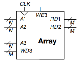
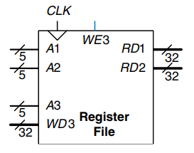
Multiported memories can access several addresses simultaneously. The figure shows a three-ported memory with two read ports and one write port. Port 1 reads the data from address A1 onto the read data output RD1. Port 2 reads the data from address A2 onto RD2. Port 3 writes the data from the write data input, WD3, into address A3 on the rising edge of the clock if the write enable, WE3, is asserted.
Memory Types
Memory arrays are specified by their size (depth width) and the number and type of ports. All memory arrays store data as an array of bit cells, but they differ in how they store bits.
Memories are classified based on how they store bits in the bit cell. The broadest classification is random access memory (RAM) versus read only memory (ROM). RAM is volatile, meaning that it retains its data indefinitely, even without a power source.
RAM and ROM received their names for historical reasons that are no longer very meaningful. RAM is called random access memory because any data word is accessed with the same delay as any other. A sequential access memory, such as a tape recorder, accesses nearby data more quickly than faraway data.
ROM is called read only memory because, historically, it could only be read but not written. These names are confusing, because ROMs are randomly accessed too. Worse yet, most modern ROMs can be written as well as read! The important distinction to remember is that RAMs are volatile and ROMs are nonvolatile.
The two major types of RAMs are dynamic RAM (DRAM) and static RAM (SRAM). Dynamic RAM stores data as a charge on a capacitor, whereas static RAM stores data using a pair of cross-coupled inverters. There are many flavors of ROMs that vary by how they are written and erased.
Dynamic Random Access Memory
Dynamic RAM (DRAM) stores a bit as the presence or absence of charge on a capacitor. The figure shows a DRAM bit cell. The bit value is stored on a capacitor. The nMOS transistor behaves as a switch that either connects or disconnects the capacitor from the bitline. When the wordline is asserted, the nMOS transistor turns ON, and the stored bit value transfers to or from the bitline.
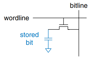
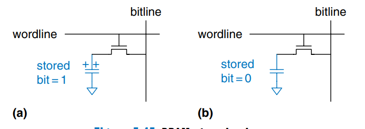
As shown in a), when the capacitor is charged to , the stored bit is 1; when it is discharged to GND as shown in b), the stored bit is 0. The capacitor node is dynamic because it is not actively driven HIGH or LOW by a transistor tied to or GND.
Upon a read, data values are transferred from the capacitor to the bitline. Upon a write, data values are transferred from the bitline to the capacitor. Reading destroys the bit value stored on the capacitor, so the data word must be restored (rewritten) after each read. Even when DRAM is not read, the contents must be refreshed (read and rewritten) every few milliseconds, because the charge on the capacitor gradually leaks away.
Static Random Access Memory (SRAM)
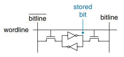
Static RAM (SRAM) is static because stored bits do not need to be refreshed. The figure shows an SRAM bit cell. The data bit is stored on cross-coupled inverters like those descibed earlier. Each cell has two outputs, bitline and . When the wordline is asserted, both nMOS transistors turn on, and data values are transferred to or from the bitlines. Unlike DRAM, if noise degrades the value of the stored bit, the cross-coupled inverters restore the value.
Area and Delay
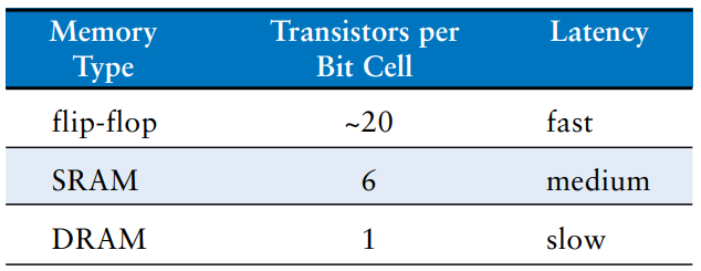
Flip-flops, SRAMs and DRAMs are all volatile memories, but each has different area and delay characteristics. The table shows a comparison of these three types of volatile memory. The data bit stored in a flip-flop is available immediately at its output. But flip-flops take at least 20 transistors to build. Generally, the more transistors a device has, the more area, power, and cost it requires. DRAM latency is longer than that of SRAM because its bitline is not actively driven by a transistor. DRAM must wait for charge to move (relatively) slowly from the capacitor to the bitline. DRAM also has lower throughput than SRAM, because it must refresh data periodically and after a read.
Memory latency and throughput also depend on the memory size; larger memories tend to be slower than smaller ones if all else is the same. The best memory type for a particular design depends on the speed, cost and power constraints.
Register Files
Digital systems often use a number of registers too store temporary variables. This group of registers, called a register file, is usually built as a small, multiported SRAM array, because it is more compact than an array of flip-flops.
The figure shows a 32-register 32-bit three-ported register file built from a three-ported memory. The register file has two read ports and one write port. The 5-bit addresses can each access all registers. So, two registers can be read and one register written simultaneously.
Read Only Memory
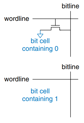
Read only memory (ROM) stores a bit as the presence or absence of a transistor. The figure shows a simple ROM bit cell. To read the cell, the bitline is weakly pulled HIGH. Then the wordline is turned ON. If the transistor is present, it pulls the bitline LOW. If it is absent, the bitline remains HIGH. Note that the ROM bit cell is a combinational circuit and has no state to “forget” if power is turned off.
The contents of a ROM can be indicated using dot notation. The figure shows the dot notation for a 4-word 3-bit ROM. A dot at the intersection of a row (wordline) and a column (bitline) indicates that the data bit is 1. For example, the top wordline has a single dot on , so the data word at Address 11 is 010.
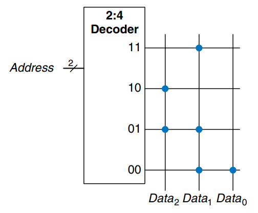
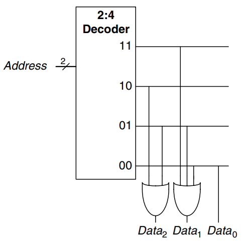
Conceptually, ROMs can be built using two-level logic with a group of gates followed by a group of gates. The gates produce all possible minterms and hence form a decoder. The figure shows the ROM from above built using a decoder and gate. Each dotted row in the above figure is an input to an gate in this figure. For data bits with a single dot, in this case , no gate is needed. This representation of a ROM is interesting because it shows how the ROM can perform any two-level logic function. In practice, ROMs are built from transistors instead of logic gates, to reduce their size and cost.
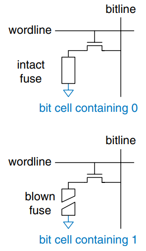
The contents of the ROM bit cell above are specified during manufacturing by the presence or absence of a transistor in each bit cell. A programmable ROM (PROM) places a transistor in every bit cell but provides a way to connect or disconnect the transistor to ground.
The figure shows the bit cell for a fuse-programmable ROM. The user programs the ROM by applying a high voltage to selectively blow fuses. If the fuse is present, the transistor is connected to GND and the cell holds a 0. If the fuse is destroyed, the transistor is disconnected from ground and the cell holds a 1. This is also called a one-time programmable ROM, because the fuse cannot be repaired once it is blown.
Reprogrammable ROMs provide a reversible mechanism for connecting or disconnecting the transistor to GND. Erasable PROMs (EPROMs) replace the nMOS transistor and fuse with a floating-gate transistor. The floating gate is not physically attached to any other wires. When suitable high voltages are applied, electrons tunnel through an insulator onto the floating gate, turning on the transistor and connecting the bitline to the wordline (decoder output). When the EPROM is exposed to intense ultraviolet light for about half an hour, the electrons are knocked off the floating gate, turning the transistor off. These actions are called programming and erasing, respectively. Electrically erasable PROMs (EEPROMs) and Flash memory use similar principles but include circuitry on the chip for erasing as well as programming, so no UV light is necessary. EEPROM bit cells are individually erasable; Flash memory erases larger blocks of bits and is cheaper because fewer erasing circuits are needed. In 2006, Flash memory cost less than 25 dollars per GB, and the price continued to drop by 40% a year. Flash had become an extremely popular way to store large amounts of data in portable battery-powered systems such as cameras and USB sticks.
In summary, modern ROMs are not really read only; they can be programmed as well. The difference between RAM and ROM is that ROMs take a longer time to write but are nonvolatile.
Logic Using Memory Arrays
Although they are used primarily for data storage, memory array can also perform combinational logic, For example, the output of the ROM above is the of the two Address inputs. Likewise, is the of the two inputs. A -word -bit memory can perform any combinational function of inputs and outputs.
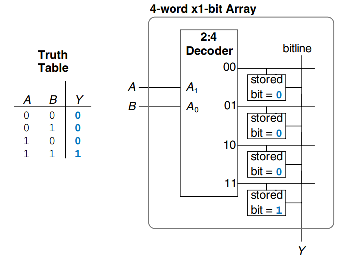
Memory arrays used to perform logic are called lookup tables (LUTs). The figure shows a 4-word 1-bit memory array used a a lookup table to perform the function . Using memory to perform logic, the user can look up the output value for a given input combination (address). Each address corresponds to a row in the truth table, and each data bit corresponds to an output value.
Memory HDL
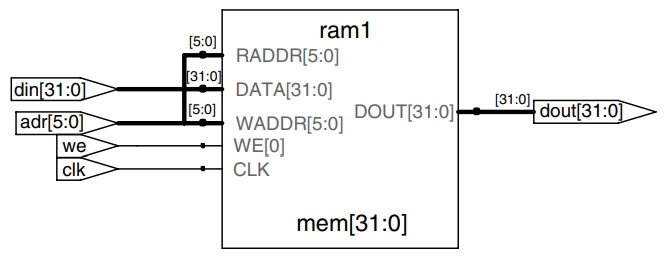
The example describes a -word -bit RAM. the RAM has a synchronous enabled write. In other words, writes occur on the rising edge of the clock if the write enable, , is asserted. Reads occur immediately. When power is first applied, the contents of the RAM are unpredictable.
module ram # (parameter N = 6, M = 32)
             (input          clk,
              input          we,
              input  [N-1:0] adr,
              input  [M-1:0] din,
              output [M-1:0] dout);
  reg [M-1:0] mem [2**N-1:0];
  always @ (posedge clk)
    if (we) mem [adr] <= din;
  assign dout = mem[adr];
endmodule
This example describes a 4-word 3-bit ROM. The contents of the ROM are specified in the HDL case statement. A ROM as small as this one may be synthesized into logic gates rather than an array. Note that the seven-segment decoder from earlier synthesizes into a ROM.
module rom (input      [1:0] adr,
            output reg [2:0] dout);
  always @ (adr)
    case (adr)
      2b00: dout  3b011;
      2b01: dout  3b110;
      2b10: dout  3b100;
      2b11: dout  3b010;
    endcase
endmodule
Logic Arrays
Like memory, gates can be organized into regular arrays. If the connections are made programmable, these logic arrays can be configured to perform any function without the user having to connect wires in specific ways. The regular structure simplifies design. Logic arrays are mass produced in large quantities, so they are inexpensive. Software tools allow users to map logic designs onto these arrays. Most logic arrays are also reconfigurable, allowing designs to be modified without replacing the hardware. Reconfigurability is valuable during development and is also useful in the field, because a system can be upgraded by simply downloading the new configuration.
This section introduces two types of logic arrays: programmable logic arrays (PLAs), and field programmable gate arrays (FPGAs). PLAs, the older technology, perform only combinational logic functions. FPGAs can perform both combinational and sequential logic.
Programmable Logic Array
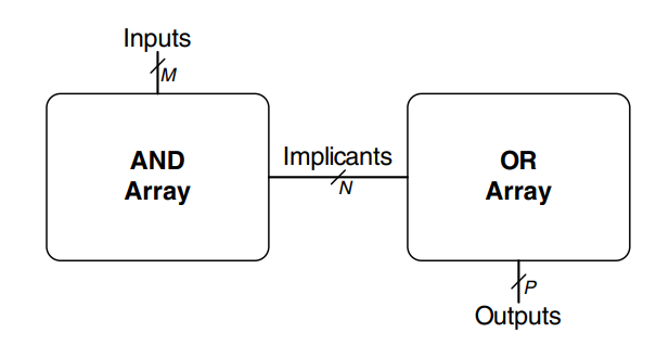
Programmable logic arrays (PLAs) implement two-level combinational logic in sum-of-products (SOP) form. PLAs are built from an array followed by an array, as shown. The inputs (in true and complementary form) drive an array, which produces implicants, which in turn are -ed together to form the outputs. An -bit PLA has inputs, implicants and outputs.
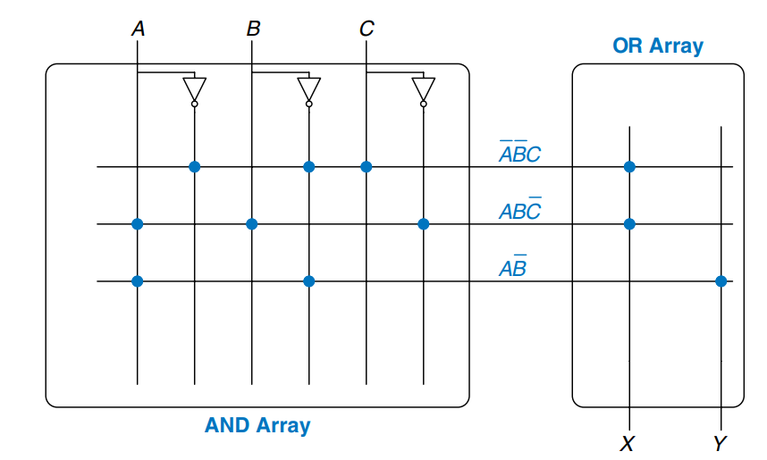
The figure shows the dot notation for a -bit PLA performing the functions and . Each row in the array forms an implicant. Dots in each row of the array indicate which literals comprise the implicant. The array in the figure forms three implicants: , , and . Dots in the array indicate which implicants are part of the output function.
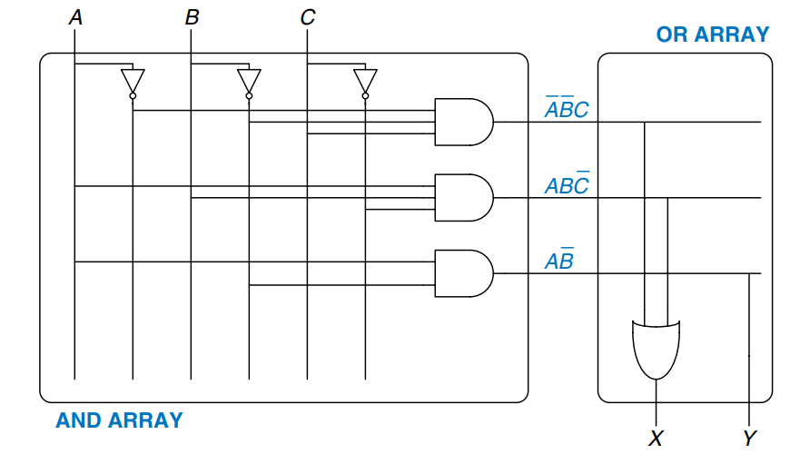
This figure shows how PLAs can be built using two-level logic.
ROMs can be viewed as a special case of PLAs. A -word -bit ROM is simply an -bit PLA. The decoder behaves as an plane that produces the outputs. If the function does not depend on all minterms, a PLA is likely to be smaller than a ROM. For example, an 8-word 2-bit ROM is required to perform the same functions performed by the -bit PLA shown.
Programmable logic devices (PLDs) are souped-up PLAs that add registers and various other features to the basic planes. However, PLDs and PLAs have largely been displaced by FPGAs, which are more flexible and efficient for building large systems.
Field Programmable Gate Array
A field programmable gate array (FPGA) is an array of reconfigurable gates. Using software programming tools, a user can implement designs on the FPGA using either an HDL or a schematic. FPGAs are more powerful and more flexible than PLAs for several reasons. They can implement both combinational and sequential logic. They can also implement multilevel logic functions, whereas PLAs can only implement two-level logic. Modern FPGAs integrate other useful functions such as built-in multipliers and large RAM arrays.
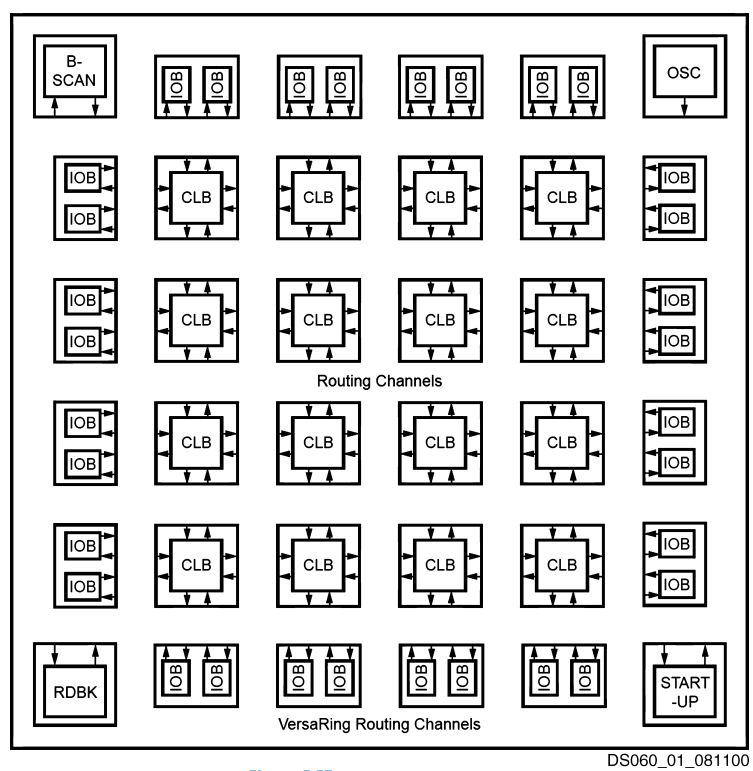
FPGAs are built as an array of configurable logic blocks (CLBs). The figure shows the block diagram of the Spartan FPGA introduced by Xilinx in 1998. Each CLB can be configured to perform combinational or sequential functions. The CLBs are surrounded by input/output blocks (IOBs) for interfacing with external devices. The IOBs connect CLB inputs and outputs to pins on the chip package. CLBs can connect to other CLBs and IOBs through programmable routing channels. The remaining blocks shown in the figure aid in programming the device.
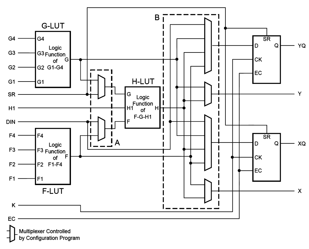
The figure shows a single CLB for the Spartan FPGA. Other brands of FPGAs are organized somewhat differently, but the same general principles apply. The CLB contains lookup tables (LUTs), configurable multiplexers, and registers. The FPGA is configured by specifying the contents of the lookup tables and the select signals for the multiplexers.
Each Spartan CLB has three LUTs: the four-input F- and G-LUTs, and the three-input H-LUT. By loading the appropriate values into the lookup tables, the F- and G-LUTs can each be configured to perform any function of up to four variables, and the H-LUT can perform any function of up to three variables.
Configuring the FPGA also involves choosing the select signals that determine how the multiplexers route data through the CLB. For example, depending on the multiplexer configuration, the H-LUT may receive on eof its inputs from either DIN or the F-LUT. Similarly, it receives another input from either SR or the G-LUT. The third input always comes from H1.
The FPGA produces two combinational outputs, and . Depending on the multiplexer configuration, comes from either the F- or H-LUT. comes from either the G- or H-LUT. These outputs can be connected to other CLBs via the routing channels.
The CLB also contains two flip-flops. Depending on the configuration, the flip-flop inputs may come from DIN or from the F-, G- or H-LUT. The flip-flop outputs, and , can also be connected to other CLBs via the routing channels.
In summary, the CLB can perform up to two combinational and/or two registered functions. All of the functions can involve at least four variables, and some can involve up to nine.
The designer configures an FPGA by first creating a schematic or HDL description of the design. The design is the synthesized onto the FPGA. The synthesis tool determines how the LUTs, multiplexers, and routing channels should be configured to perform the specified functions. This configuration information is the downloaded to the FPGA.
Because Xilinx FPGAs store their configuration information in SRAM, they can easily be reprogrammed. They may download the SRAM contents from a computer in the laboratory or from an EEPROM chip when the system is turned on. Some manufacturers include EEPROM directly on the FPGA or use one-time programmable fuses to configure the FPGA.
Array Implementations
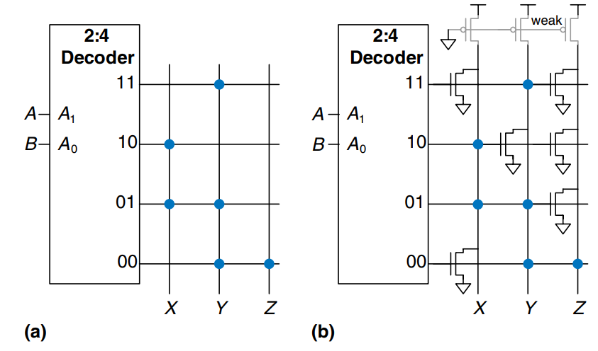
To minimize their size and cost, ROMs and PLAs commonly use pseudo-nMOS or dynamic circuits instead of conventional logic gates. Figure a) shows the dot notation for a 4 3-bit ROM that performs the following functions: , , and . The pseudo-nMOS implementation is given in b). Each decoder output is connected to the gates of the nMOS transistors in its row. Remember that in pseudo-nMOS circuits, the weak pMOS transistor pulls the output HIGH only if there is no path to GND through the pull-down (nMOS) network.
Pull-down transistors are placed at every junction without a dot. The dots from the dot notation diagram of a) are left faintly visible in b) for easy comparison. The weak pull-up transistors pull the output HIGH for each wordline without a pull-down transistor.
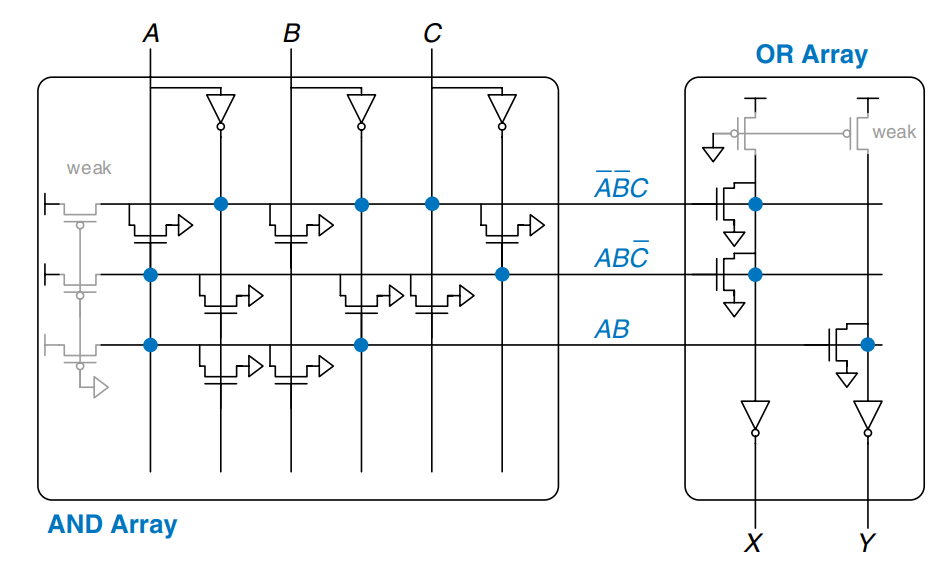
PLAs can also be built using pseudo-nMOS circuits, as shown in the figure. Pull-down (nMOS) transistors are placed on the complement of dotted literals in the array and on dotted rows in the array. The columns in the array are sent through an inverter before they are fed to the output bits. Again, the blue dots from the dot notation diagram are left faintly visible for easy comparison.
